A jumping cap circuit and its design method
A design method and circuit technology, applied in the direction of CAD circuit design, logic circuit interface device, logic circuit connection/interface layout, etc., can solve the problem that the chip cannot work normally, and achieve the effect of improving reliability and realizing the circuit.
- Summary
- Abstract
- Description
- Claims
- Application Information
AI Technical Summary
Problems solved by technology
Method used
Image


Examples
Embodiment 1
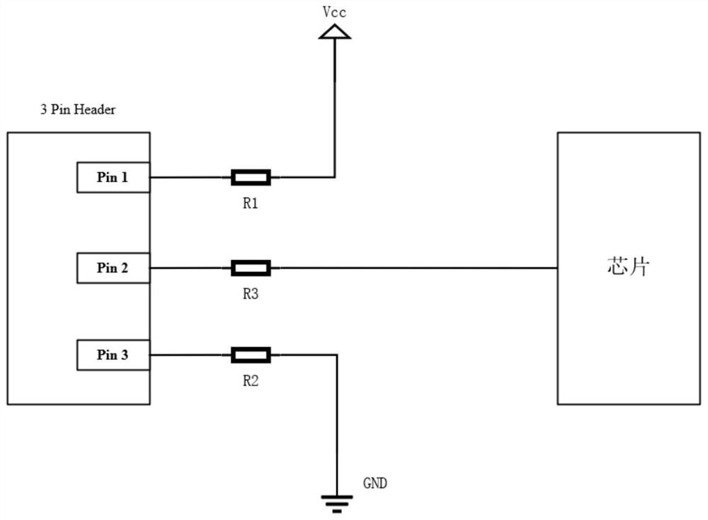
[0038] see figure 2 , figure 2 It is a schematic circuit schematic diagram of a jumping cap circuit provided in the embodiment of the present application. Depend on figure 2 It can be seen that the jumper circuit of this embodiment includes a 3-pin pin header and a chip, and also includes a pull-up resistor R2, and the pin header is connected to the chip through the pull-up resistor R2. figure 2 Among them, pin1 is the first pin, pin2 is the second pin, pin3 is the third pin, resistor R1 is connected to the first pin, R2 is a pull-up resistor, pull-up resistor R2 is connected to the second pin, and resistor R3 is connected to the third pin connect.
[0039] In the jumper circuit of this embodiment, the default input state of the chip is high level. The first pin is grounded through the resistor R1, and the second pin is pulled high by the pull-up R2 and then connected to the chip. The resistance value relationship between the resistor R1 and the pull-up resistor R2 is...
Embodiment 2
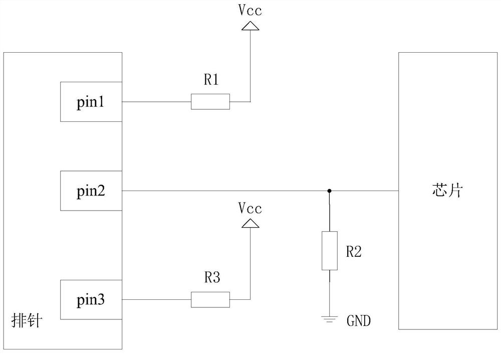
[0048] exist figure 2 On the basis of the illustrated embodiment see image 3 , image 3 It is a schematic circuit schematic diagram of another jumping cap circuit provided in the embodiment of the present application. Depend on image 3 It can be seen that the jumper circuit of this embodiment also includes a 3pin pin header and a chip, and also includes a pull-down resistor R2 and a resistor R1 that divides the voltage with the pull-down resistor R2. The pin header is connected to the chip through the pull-down resistor R2. The first pin is pulled up to Vcc through resistor R1. image 3 Among them, pin1 is the first pin, pin2 is the second pin, pin3 is the third pin, resistor R1 is connected to the first pin, R2 is a pull-down resistor, pull-down resistor R2 is connected to the second pin, and resistor R3 is connected to the third pin.
[0049] The default input state of the chip in the jumper circuit of this embodiment is low level. The first pin is pulled high by the...
Embodiment 3
[0056] exist figure 2 and image 3 On the basis of the illustrated embodiment see Figure 4 , Figure 4 It is a schematic flowchart of a design method of a jumper cap circuit provided in the embodiment of the present application. Depend on Figure 4 As can be seen, the design method of the jump cap circuit in the present application mainly includes:
[0057] S1: Obtain the default input state of the chip, where the default input state of the chip includes high level and low level.
[0058] This application is mainly applicable to a jumper circuit including a chip and a 3pin header.
[0059] S2: According to the default input state of the chip, set the default value of the chip by setting the first resistor on the line where the first pin of the pin header is located, and setting the second resistor on the line where the second pin of the pin header is located. value. Among them, the default value of the chip includes logic 0 or logic 1, the second resistor is a pull-up...
PUM
 Abstract
Description
Claims
Application Information
 - R&D
- Intellectual Property
- Life Sciences
- Materials
- Tech Scout
- Unparalleled Data Quality
- Higher Quality Content
- 60% Fewer Hallucinations
Browse by: Latest US Patents, China's latest patents, Technical Efficacy Thesaurus, Application Domain, Technology Topic, Popular Technical Reports.
© 2025 PatSnap. All rights reserved.Legal|Privacy policy|Modern Slavery Act Transparency Statement|Sitemap|About US| Contact US: help@patsnap.com