
Display panel and display device

A display panel and substrate substrate technology, applied in character and pattern recognition, print image acquisition, instruments, etc., can solve the problem of low fingerprint recognition accuracy, achieve the effect of improving core competitiveness and simple preparation process

Active Publication Date: 2021-01-12
WUHAN TIANMA MICRO ELECTRONICS CO LTD
View PDF6 Cites 0 Cited by
  • Summary
  • Abstract
  • Description
  • Claims
  • Application Information

AI Technical Summary

Problems solved by technology

[0004] However, in the existing display panels, how to overcome the problem of low fingerprint recognition accuracy of the display panel and design a display panel with higher fingerprint recognition accuracy is a major problem faced by the industry

Method used


Image

  • Display panel and display device
  • Display panel and display device
  • Display panel and display device

Examples


Embodiment Construction

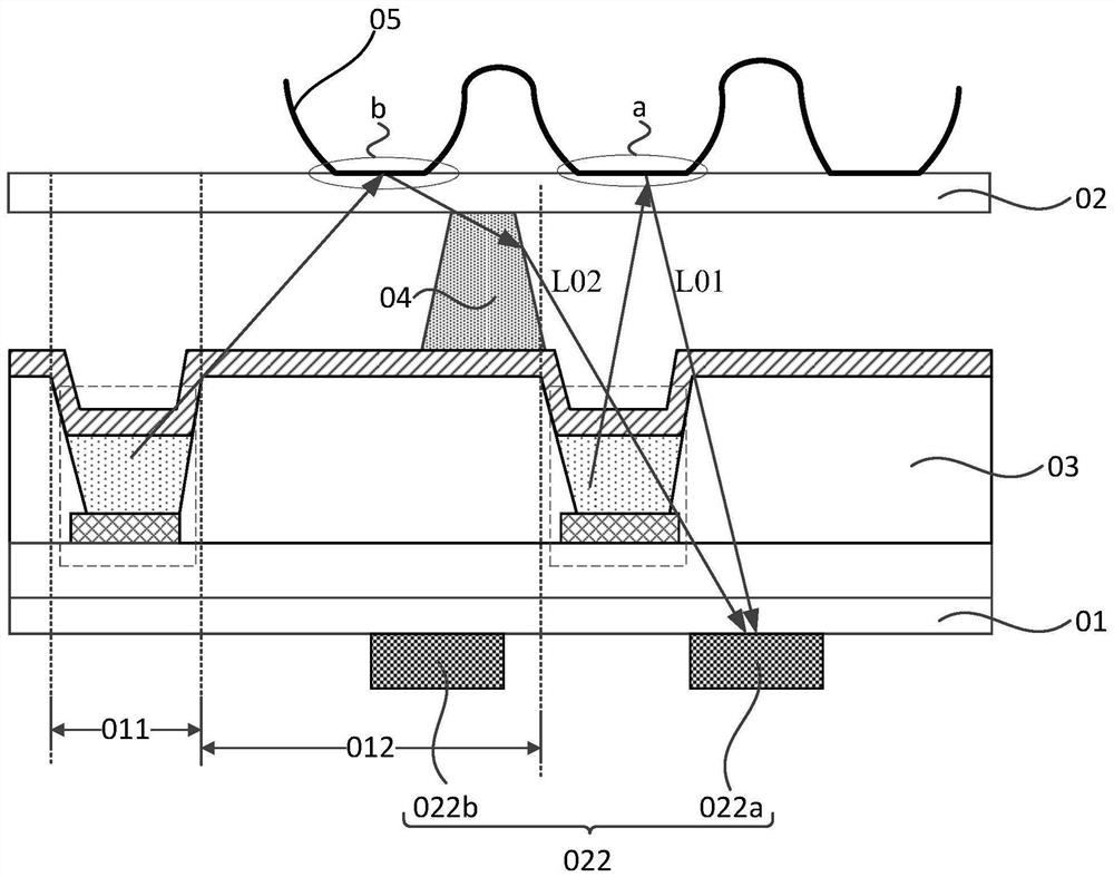
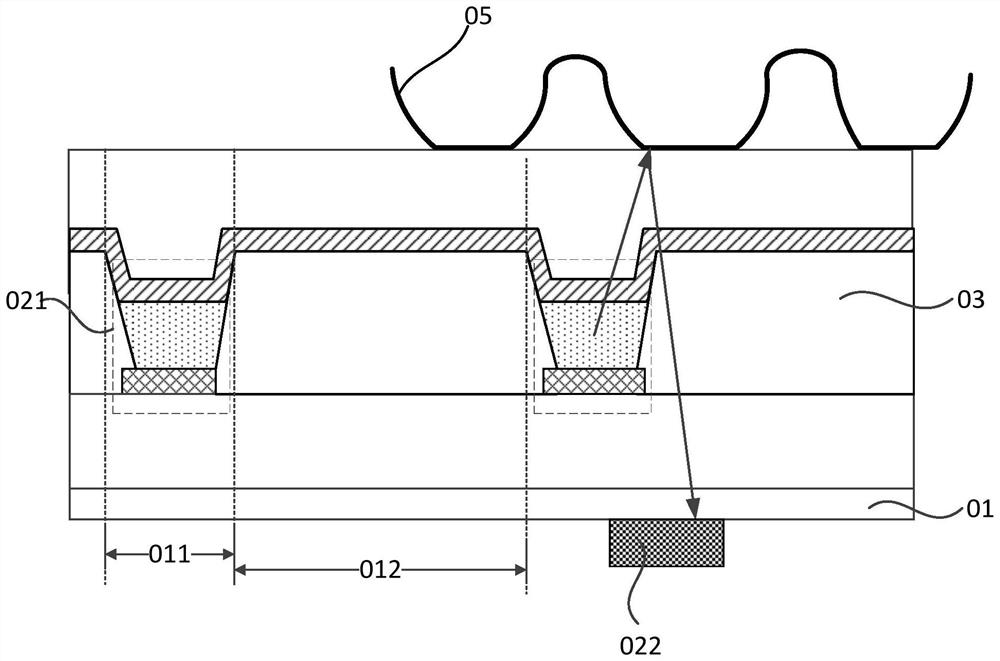
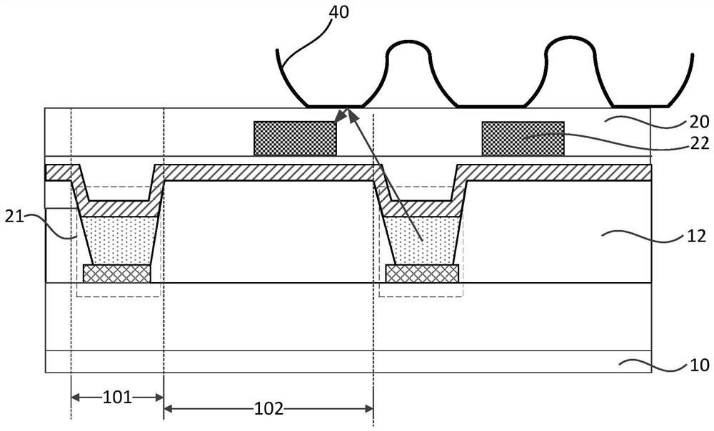
[0025] The present invention will be further described in detail below in conjunction with the accompanying drawings and embodiments. It should be understood that the specific embodiments described here are only used to explain the present invention, but not to limit the present invention. In addition, it should be noted that, for the convenience of description, only some structures related to the present invention are shown in the drawings but not all structures.

[0026] In any embodiment of the present invention, the display panel includes a fingerprint identification light source. In actual setting, the light emitting unit in the display panel can be reused as a fingerprint recognition light source, or an external light source can be used as a fingerprint recognition light source. This application is not limited to this. For ease of understanding, in each figure, the formation and propagation path of fingerprint signal light are drawn by taking the multiplexing of the li...


PUM


Abstract

The embodiment of the invention discloses a display panel and a display device. The display panel includes: a base substrate, including a plurality of opening areas and a non-opening area surrounding the opening areas; a pixel defining layer formed on the base substrate, and the pixel defining layer is on the base substrate The vertical projection of is located in the non-opening area; the thin film encapsulation layer formed on the side of the pixel defining layer away from the base substrate; and the fingerprint signal acquisition module, the fingerprint signal acquisition module is located in any of the following positions One, between the pixel defining layer and the thin film encapsulating layer, the side of the thin film encapsulating layer away from the pixel defining layer, and the inside of the thin film encapsulating layer. The display panel provided by the embodiment of the present invention can improve the fingerprint identification accuracy of the display panel.

Description

technical field [0001] The embodiments of the present invention relate to the field of display technology, and in particular to a display panel and a display device with a fingerprint recognition function. Background technique [0002] Each person's skin texture, including fingerprints, varies in patterns, breakpoints, and intersections, which are unique and remain unchanged throughout life. Accordingly, we can match a person with his fingerprint, and verify his real identity by comparing his fingerprint with the pre-saved fingerprint data. This is fingerprint recognition technology. Thanks to electronic integrated manufacturing technology and fast and reliable algorithm research, optical fingerprint recognition technology in fingerprint recognition technology has begun to enter our daily life, and has become the most in-depth research, the most widely used and the most mature in biometrics. technology. [0003] At present, the optical fingerprint identification technology...

Claims


Application Information

Patent Timeline
Patent Type & Authority Patents(China)
IPC IPC(8): G06K9/00
CPCG06V40/1318
Inventor 李波
Owner WUHAN TIANMA MICRO ELECTRONICS CO LTD
Learn More