A System-on-Chip Based on Two-Level Boot Structure

A system-level chip and connecting chip technology, which is applied in the direction of instruments, calculations, and electrical digital data processing, can solve the problems of no address input, the processor cannot randomly fetch instructions to access, and no discovery, etc., so as to save time and be very reliable. Effects of portability and versatility, improved verifiability and testability

Active Publication Date: 2022-03-22
XIAN MICROELECTRONICS TECH INST
View PDF8 Cites 0 Cited by
  • Summary
  • Abstract
  • Description
  • Claims
  • Application Information

AI Technical Summary

Problems solved by technology

The second method is mostly used when the SoC is externally connected to a serial PROM and other non-randomly readable memory as a program storage area. This type of memory bank has no address input and can only output data serially according to the input clock, and the processor cannot randomly fetch instructions. Access to this type of storage, so the program in the program storage area can only be moved to other program execution areas that can be randomly fetched through the on-chip BOOT boot mechanism to achieve loading and startup
[0005] At present, there are many patents on the BOOT method. However, there is no design structure compatible with serial memory BOOT loading, parallel memory BOOT loading, and NOBOOT direct execution.

Method used


Image

  • A System-on-Chip Based on Two-Level Boot Structure
  • A System-on-Chip Based on Two-Level Boot Structure
  • A System-on-Chip Based on Two-Level Boot Structure

Examples


Embodiment Construction

[0021] The technical solutions of the present invention will be further described below with reference to the accompanying drawings and specific examples.

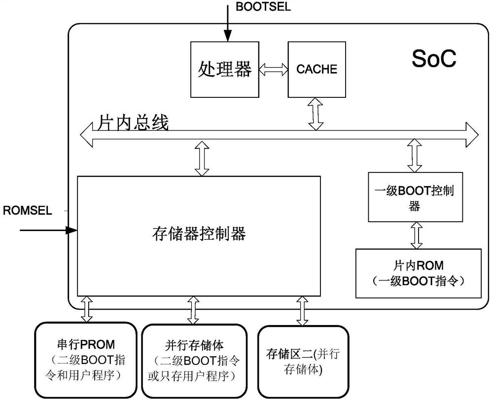
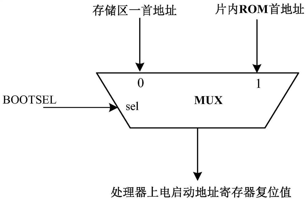
[0022] The present invention provides a system-level chip based on a two-stage BOOT structure, such as figure 1 As shown, including a memory controller, a memory controller connecting piece, a cache memory (Cache) between the in-chip buses and the processor, and the in-chip boke is set between the slide ROM; memory The controller connects two external storage area one and storage area two, where the storage area includes a serial PROM and parallel MRAM, and the memory controller can only access one of the one; the storage area is parallel SRAM. Where the processor is connected to the Bootsel control pin, the memory controller is connected to the ROMSEL control pin.

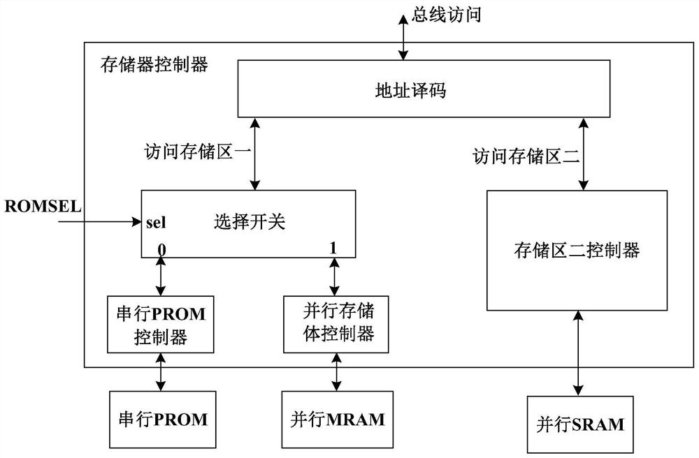
[0023] Such as image 3 As shown, the memory controller includes an address decoding unit connected to a sheet bus, and an address decoding unit is connected to a ...


PUM


Abstract

The invention discloses a system-level chip based on a two-level BOOT structure, which includes a memory controller connected to a processor through an on-chip bus, and connected to an on-chip ROM through an on-chip bus; wherein the memory controller is connected to storage area 1 and storage Area two; storage area one includes serial PROM and parallel MRAM, and the memory controller accesses serial PROM or parallel MRAM at the same time; storage area two is parallel SRAM; where the on-chip ROM stores a first-level BOOT instruction, and the processor accesses The content stored in the on-chip ROM; the storage area 1 stores the secondary BOOT instructions and user programs; the processor is connected to the BOOTSEL control pin; the memory controller is connected to the ROMSEL control pin. The start address of power-on reset and the type of off-chip storage to be accessed are selected by hardware control, and three power-on start modes of the system-level chip are realized based on the two-level BOOT structure.

Description

Technical field [0001] The present invention belongs to the field of integrated circuit design; specifically, a system-level chip based on a two-stage BOOT structure. Background technique [0002] The existing SOC power-on launch mainly uses two methods: First, SOC externally read non-volatile devices as program memory, after power-on reset, SOC reads instruction execution programs directly from the program memory; second The SOC will divide three regions including the in-chip and the outer storage, respectively, for the boot boot area, program storage area, and program execution area. After power-on reset, the SOC executes the instructions in the boot boot area to carry the content of the storage area. To the execution zone, then jump to the program execution area to execute the user program. [0003] In the above two methods, the first method is suitable for the case where the SOC external flash or MRAM can be randomly read as the program area, and these type memory supports SO...

Claims


Application Information

Patent Timeline
Patent Type & Authority Patents(China)
IPC IPC(8): G06F30/398G06F13/16
CPCG06F13/1668G06F30/398
Inventor 罗敏涛赵翠华张春妹刘思源杨博
Owner XIAN MICROELECTRONICS TECH INST
Why Eureka
Try Eureka