A kind of manufacturing method and product of cof single-sided flexible substrate fine circuit
A flexible substrate, manufacturing method technology, applied in the exposure method of radiation-sensitive mask, printed circuit manufacturing, removing conductive material by chemical/electrolytic method, etc., can solve the minimum line width/line spacing not reaching 10 microns, etc. question
- Summary
- Abstract
- Description
- Claims
- Application Information
AI Technical Summary
Problems solved by technology
Method used
Image
Examples
Embodiment 1
[0028] COF single-sided flexible substrate fine lines are made by the following steps:
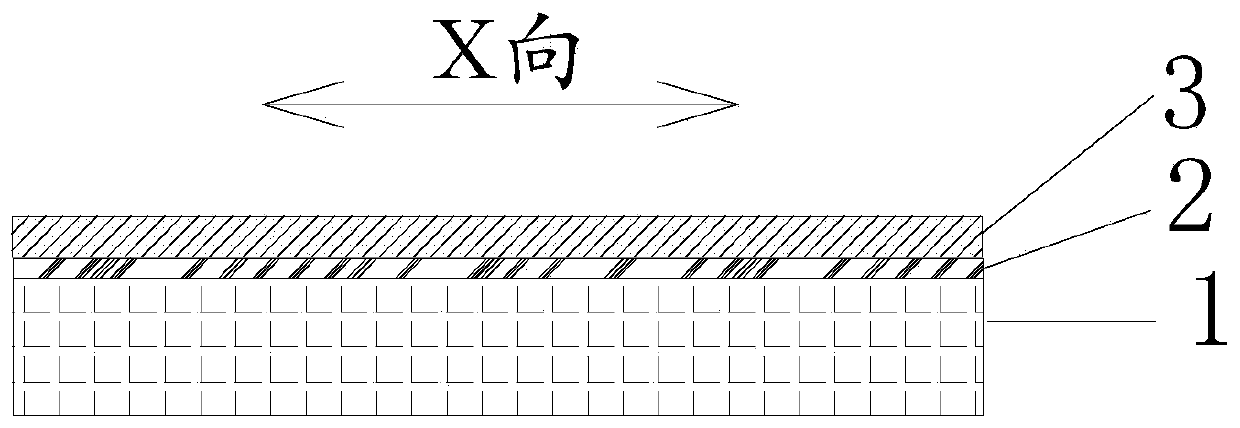
[0029] (1) Dry film lamination: a metal Ni / Cr layer 2 with a thickness of 20 nanometers is arranged on the upper surface of the polyimide lower layer 1, and a copper layer 3 with a thickness of 1 micrometer is arranged on the upper surface of the metal Ni / Cr layer 2 A base material is made, and a dry film with a thickness of 15 microns is formed by vacuum pressing on the upper surface of the copper layer 3;
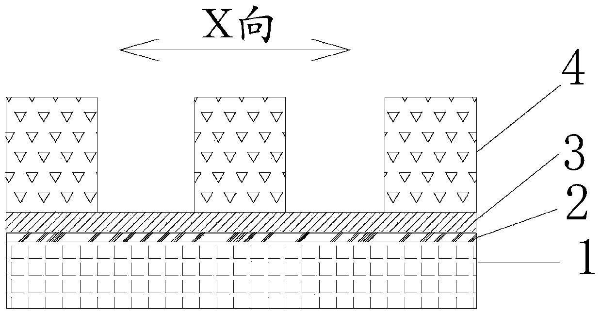
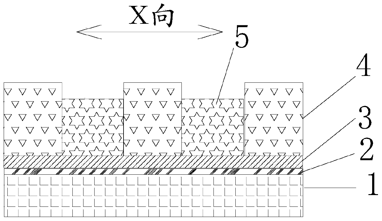
[0030] (2) UV exposure of dry film: cover the glass negative film on the dry film, the glass negative film includes a transparent area and a black area spaced apart in the X direction, the X dimension of each transparent area is 5 microns, and each black area is 5 microns. The X dimension of the area is 9 microns. The dry film covered with the glass negative is irradiated and exposed by ultraviolet rays, and the glass negative is removed. The part covered by the transparent area on th...
Embodiment 2
[0038] The difference from Example 1 is: in step (2), the X dimension of each transparent area and the dry film exposed part 4 is 4 microns, and the X dimension of each black area and the dry film unexposed part is 10 μm. microns.
Embodiment 3
[0040] The difference from Example 1 is: in step (1), the thickness of the copper layer 3 is 0.5 microns; in step (2), the X dimension of each transparent area and the dry film exposure part 4 is 6 microns, and each Both the black area and the unexposed portion of the dry film had an X dimension of 8 microns.
PUM
| Property | Measurement | Unit |
|---|---|---|
| thickness | aaaaa | aaaaa |
| thickness | aaaaa | aaaaa |
| thickness | aaaaa | aaaaa |
Abstract
Description
Claims
Application Information
 - R&D Engineer
- R&D Manager
- IP Professional
- Industry Leading Data Capabilities
- Powerful AI technology
- Patent DNA Extraction
Browse by: Latest US Patents, China's latest patents, Technical Efficacy Thesaurus, Application Domain, Technology Topic, Popular Technical Reports.
© 2024 PatSnap. All rights reserved.Legal|Privacy policy|Modern Slavery Act Transparency Statement|Sitemap|About US| Contact US: help@patsnap.com


