Preparation method of thin-film resistor

A technology of thin-film resistors and metal electrodes, which is applied in the direction of resistors, circuits, electrical components, etc., can solve the problems of reducing the reliability of thin-film resistors and affecting the accuracy of thin-film resistors, and achieve the effects of improving accuracy and reliability and avoiding over-etching

Inactive Publication Date: 2018-09-28
SHANGHAI INTEGRATED CIRCUIT RES & DEV CENT
View PDF10 Cites 2 Cited by
  • Summary
  • Abstract
  • Description
  • Claims
  • Application Information

AI Technical Summary

Problems solved by technology

In this prior art, since the electrode material is etched by a dry etching process, an additional amount of overetching needs to be added in order to avoid metal electrode residue at the step, so that the thin film resistance material 102 will also be overetched at the same time, thus Affect the accuracy of thin film resistors and reduce the reliability of thin film resistors

Method used


Image

  • Preparation method of thin-film resistor
  • Preparation method of thin-film resistor
  • Preparation method of thin-film resistor

Examples


Embodiment Construction

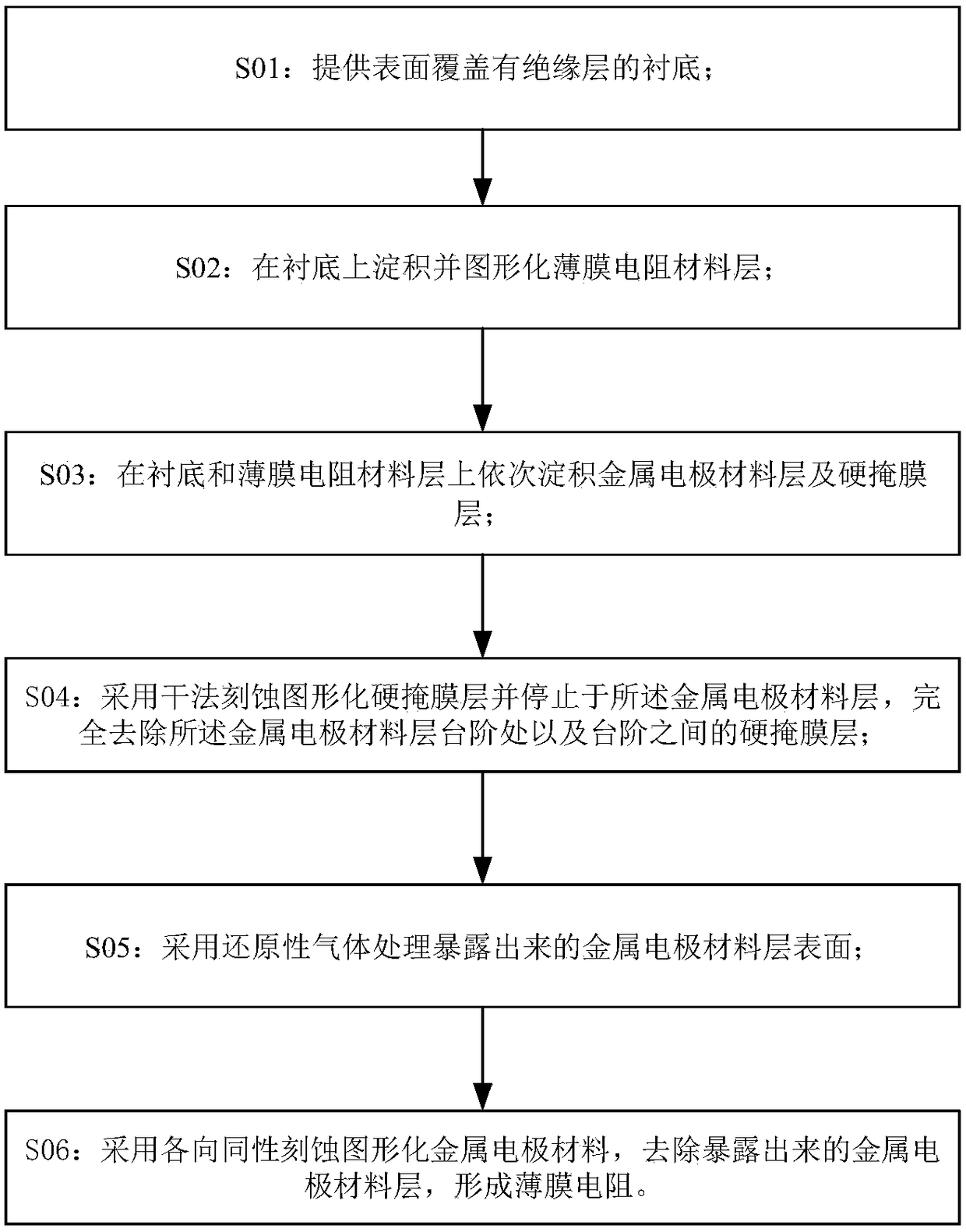
[0026] In order to make the purpose, technical solution and advantages of the present invention clearer, the specific implementation manners of the present invention will be further described in detail below in conjunction with the accompanying drawings.

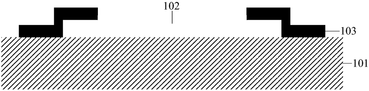
[0027] see figure 2 and image 3 , as shown in the figure is a schematic flow chart of a preferred embodiment of a method for preparing a thin film resistor of the present invention. In this embodiment, a method for preparing a thin film resistor includes the following steps:

[0028] Step S01: providing a substrate whose surface is covered with an insulating layer.

[0029] Specifically, a silicon wafer is used as a substrate, and an insulating layer is deposited on the substrate. The silicon wafer substrate may be a silicon wafer on which a CMOS processing circuit chip has been manufactured. As an optional implementation, this embodiment uses an 8-inch silicon wafer as the substrate, and deposits 3000 Angstroms of sil...


PUM

PropertyMeasurementUnit
thicknessaaaaaaaaaa
thicknessaaaaaaaaaa

Abstract

The present invention discloses a preparation method of a thin-film resistor. The method comprises the following steps: S01 providing a substrate, wherein the surface of the substrate is covered withan insulation layer; S02 depositing and graphing a thin-film resistor material layer on the substrate; S03 depositing a metal electrode material layer and a hard mask layer on the substrate and the thin-film resistor material layer successively; S04 graphing the hard mask layer by adopting dry etching, stopping on the metal electrode material layer, and removing the hard mask layer at the steps ofthe metal electrode material layer and the hard mask layer between the steps of the metal electrode material layer completely; S05 processing the surface of the exposed metal electrode material layerby adopting reducing gas(es); and S06 graphing the metal electrode material by adopting isotropic etching, and removing the exposed metal electrode material layer to form the thin-film resistor. Thepreparation method of the thin-film resistor can avoid the problems of over-etching of the thin-film resistor and etching residue of the metal electrode and improve the accuracy and the reliability ofthe thin-film resistor.

Description

technical field [0001] The invention relates to the field of semiconductor processing and manufacturing, in particular to a method for preparing a thin film resistor. Background technique [0002] As the performance requirements of modern electronic equipment are getting higher and higher, the performance requirements of on-chip components are also becoming more and more stringent. In modern large-scale integrated circuit chips and sensor chips, thin-film resistors are an indispensable device, including voltage divider resistors, thermistors, photoresistors, etc. on the chip. The accuracy of thin-film resistors also directly affects the accuracy of advanced chips. and performance. [0003] Such as figure 1 Shown is a schematic diagram of the main structure of a thin-film resistor in the prior art, and its manufacturing method mainly includes: first, providing a silicon wafer covered with an insulating layer as a substrate 101, depositing a thin-film resistor material 102 o...

Claims


Application Information

Patent Timeline
Patent Type & Authority Applications(China)
IPC IPC(8): H01L49/02
CPCH01L28/20
Inventor 左青云康晓旭李铭
Owner SHANGHAI INTEGRATED CIRCUIT RES & DEV CENT
Why Eureka
Try Eureka