Silicon wafer conveying mechanism between screen printing machine and sintering furnace

A technology of screen printing machine and conveying mechanism, which is applied in the direction of conveyor objects, furnaces, furnace components, etc., can solve the problems of increasing the fragmentation rate of solar silicon wafers, high impact force, etc., and achieve simple structure, reduce fragmentation rate, and reduce impulse force Effect

Inactive Publication Date: 2018-08-24
安徽三电光伏科技有限公司
View PDF6 Cites 0 Cited by
  • Summary
  • Abstract
  • Description
  • Claims
  • Application Information

AI Technical Summary

Problems solved by technology

However, due to the large area of ​​the conveyor belt of the sintering furnace and its width is much larger than that of the horizontal conveyor belt, a rolling arc with a larger radius is formed at the end of the conveyor belt of the sintering furnace, which makes the solar silicon wafers on the horizontal conveyor belt sinter When transported on the conveyor belt of the furnace, it will generate a large impact, which increases the fragmentation rate of solar silicon wafers

Method used


Image

  • Silicon wafer conveying mechanism between screen printing machine and sintering furnace
  • Silicon wafer conveying mechanism between screen printing machine and sintering furnace
  • Silicon wafer conveying mechanism between screen printing machine and sintering furnace

Examples


Embodiment Construction

[0028] The technical solutions of the present invention will be clearly and completely described below in conjunction with the embodiments. Apparently, the described embodiments are only some of the embodiments of the present invention, not all of them. Based on the embodiments of the present invention, all other embodiments obtained by persons of ordinary skill in the art without creative efforts fall within the protection scope of the present invention.

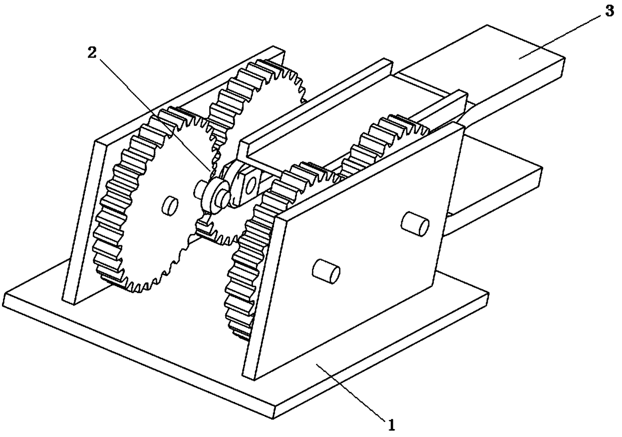
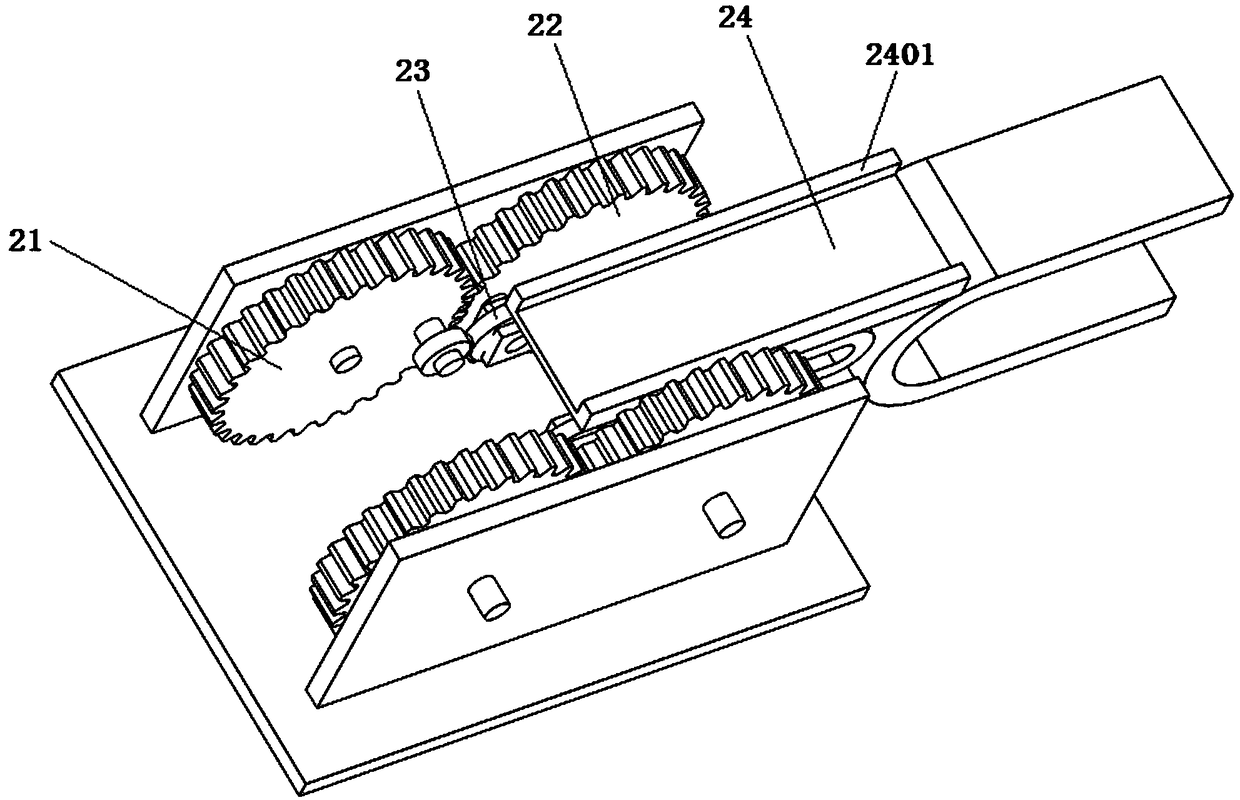
[0029] The silicon wafer conveying mechanism between the screen printing machine and the sintering furnace, such as figure 1 As shown, it includes a supporting device 1 and a feeding device 2 installed on the supporting device 1;

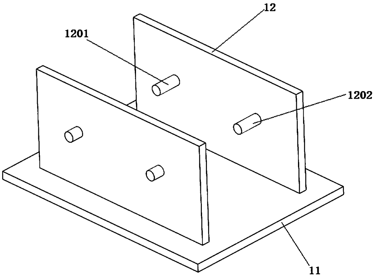
[0030] combine Figure 2 to Figure 6 As shown, the support device 1 includes a support base plate 11 and a mounting plate 12 vertically fixed on the surface of the support base plate 11, the mounting plate 12 is arranged along the length direction of the support base plate 11, and the two mounti...


PUM


Abstract

The invention discloses a silicon wafer conveying mechanism between a screen printing machine and a sintering furnace. The silicon wafer conveying mechanism comprises a supporting device and a feedingdevice, wherein the feeding device is installed on the supporting device. The supporting device comprises a supporting base plate and mounting plates, wherein the mounting plates are perpendicularlyfixed to the surface of the supporting base plate. First shaft rods and second shaft rods are fixedly arranged on the surfaces of the mounting plates in a penetrating mode. The feeding device comprises first gears, second gears, connecting rods and a feeding platform. The first gears are fixed to the surfaces of the first shaft rods, and the second gears are fixed to the surfaces of the second shaft rods. Each connecting rod comprises a strip-shaped limiting frame, and mounting rings are fixed to first stand columns. The feeding platform is fixed to the upper surfaces of the two strip-shaped limiting frames. By the adoption of the silicon wafer conveying mechanism, the impulsive force generated in the process that a solar silicon wafer is moved from the feeding platform to a conveying meshbelt of the sintering furnace can be effectively reduced, the feeding speed of the feeding platform and the conveying speed of the conveying mesh belt of the sintering furnace can be consistent, andtherefore stable and accurate conveying of the solar silicon wafer is achieved, and the wafer breakage rate is reduced.

Description

technical field [0001] The invention belongs to the technical field of solar silicon chip manufacturing, and in particular relates to a silicon chip conveying mechanism between a screen printing machine and a sintering furnace. Background technique [0002] In the screen printing process of solar silicon wafers, a printing machine is generally required to print the back electrode with silver paste on the back of the silicon wafer, and another printing machine is required to print the back field on the silicon wafer through aluminum paste, and a printing machine is also required. The positive grid is printed on the surface of the silicon wafer with silver paste, and after each printing process is completed, the solar silicon wafer needs to be transported into the sintering furnace by the conveyor belt through the screen printing output port for sintering. [0003] In the existing transportation process, a horizontal conveyor belt is generally installed at the outlet of the sc...

Claims


Application Information

Patent Timeline
Patent Type & Authority Applications(China)
IPC IPC(8): B65G49/07
CPCB65G49/07
Inventor 谢名亮
Owner 安徽三电光伏科技有限公司
Why Eureka
Try Eureka