High electrical performance chip packaging structure and manufacturing method

A technology with chip packaging structure and high electrical performance, applied in circuits, electrical components, electrical solid devices, etc., can solve the problems of inability to meet the application environment, large deformation of the solder mask, etc., to reduce the phenomenon of delamination, low cost, The effect of strong moisture resistance

Active Publication Date: 2021-06-11
HUATIAN TECH KUNSHAN ELECTRONICS
View PDF3 Cites 0 Cited by
  • Summary
  • Abstract
  • Description
  • Claims
  • Application Information

AI Technical Summary

Problems solved by technology

In other structures, there are also technical solutions in which the bottom of the opening exposes the back of the pad. Since the metal wiring layer is electrically connected to the back of the pad, its electrical performance is better, and the manufacturing process is simple. It only needs to remove the insulating layer on the back of the pad. There is no need to penetrate the welding pad; however, with this structure, experiments have proved that the stress at the corner where the metal wiring layer contacts the welding pad is relatively large. The variable is very large. Due to the pulling of the solder mask layer, the solder pad and the metal wiring layer are prone to delamination, which makes it unable to meet the higher requirements of the application environment.

Method used


Image

  • High electrical performance chip packaging structure and manufacturing method
  • High electrical performance chip packaging structure and manufacturing method
  • High electrical performance chip packaging structure and manufacturing method

Examples


Embodiment 1

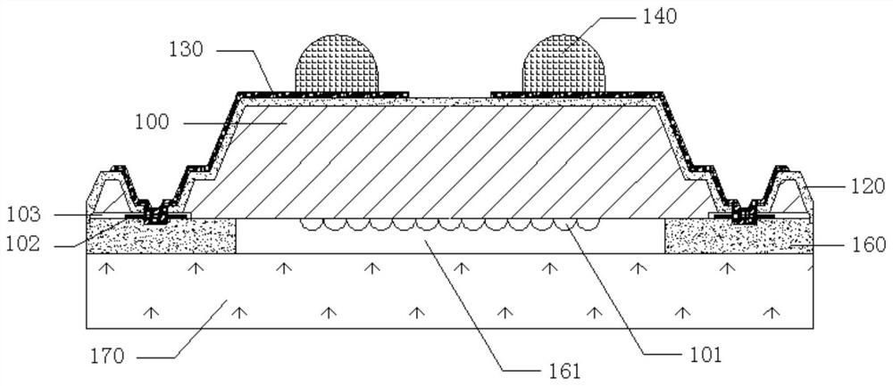
[0027] Such as figure 2As shown, a chip packaging structure with high electrical performance includes a chip 100, the front of the chip includes a functional area 101 and several soldering pads 102 located around the functional area, the front of the chip does not have a dielectric layer, and the chip The back of the substrate of the substrate is formed with a first opening 103 extending toward the pad, and the bottom of the first opening exposes the back of the pad, the back of the substrate of the chip and the sidewall of the first opening Two insulating layers 110, 120 are laid, wherein the inner insulating layer 110 is made of silicon dioxide or silicon nitride, and the outer insulating layer 120 is made of photoetching positive insulating glue. And the two layers of insulating layers extend and cover the edge of the back side of the exposed pad, and the outer layer of the insulating layer is laid with a metal wiring layer 130, and the metal wiring layer is electrically c...

Embodiment 2

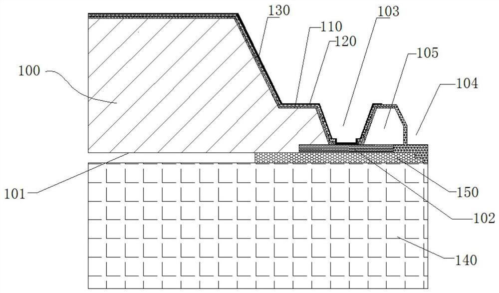
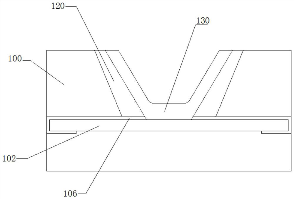
[0038] Such as image 3 with Figure 4 As shown, a chip packaging structure with high electrical performance includes a chip 100, the front side of the chip includes a functional area and several welding pads 102 located around the functional area, and a dielectric layer 106 is provided on the front side of the chip; The pad is located in the dielectric layer, and a part of the dielectric layer is separated between the pad and the substrate of the chip, and a first opening extending toward the pad is formed on the back of the substrate of the chip, and the first opening extends toward the pad. The bottom of an opening exposes the upper part of the dielectric layer on the back of the pad, and the exposed central part of the dielectric layer is hollowed out or completely hollowed out to form a second opening that exposes the back of the pad, exposing the When the central part of the dielectric layer is hollowed out, see image 3 A layer of insulating layer 120 or two layers of...


PUM


Abstract

The invention discloses a chip packaging structure with high electrical performance and a manufacturing method that can withstand the test of harsh environments. The packaging structure retains a part of the dielectric layer or adds an inorganic oxide layer on the front pad of the chip. Due to the dielectric layer or The dielectric constant of the inorganic oxide layer is low, and the experimental results show that the stress at the opening is significantly reduced, thereby reducing the delamination phenomenon between the metal wiring layer and the chip pad, and improving the packaging yield; at the same time, the inorganic oxide layer and the outer insulating layer are parallel , at the corners on the pads and at the corners of the front of the wafer and the first opening, the thickness is uniform, the dielectric constant is low, and the insulation of the product is improved, thereby preventing the occurrence of leakage failure, and the single-layer insulation layer is set in the prior art Compared with the present invention, the two insulation layers whose inner layers are inorganic oxide layers are not easily affected by moisture absorption, and have stronger moisture resistance.

Description

technical field [0001] The invention relates to the technical field of semiconductor chip packaging, in particular to a chip packaging structure with high electrical performance and a manufacturing method. Background technique [0002] figure 1 A known packaging structure of a chip is shown. The chip takes an image sensor as an example and includes an image sensor chip 100. The functional surface of the image sensor chip includes an image sensing area 101 and several pads around the image sensing area. 102; the opening, the opening extends from the back to the functional surface, and the bottom of the opening exposes the side of the pad; the metal wiring layer 130, the metal wiring layer is located on the inner wall and back of the opening, electrically connected to the pad; the insulating layer 120, The insulating layer is located between the metal wiring layer and the image sensor chip, and exposes the welding pad; a number of solder bumps 140, the solder bumps are locate...

Claims


Application Information

Patent Timeline
Patent Type & Authority Patents(China)
IPC IPC(8): H01L27/146
CPCH01L27/14636H01L27/14687
Inventor 马书英王姣郑凤霞
Owner HUATIAN TECH KUNSHAN ELECTRONICS
Why Eureka
Try Eureka