
Optical secondary module and light module

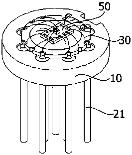
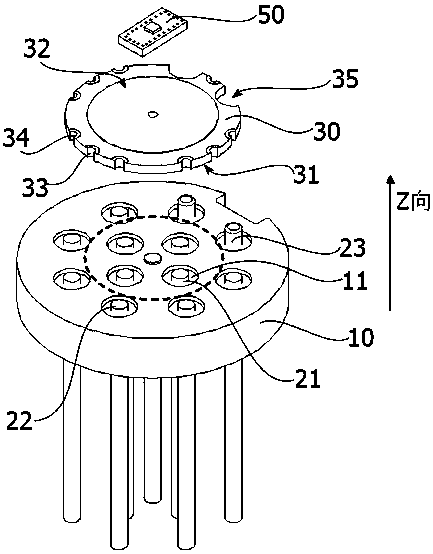
An optical sub-module and insulating board technology, applied in the field of optical communication, can solve the problem of not leaving enough space to install chips

Active Publication Date: 2018-07-27
HISENSE BROADBAND MULTIMEDIA TECH
View PDF8 Cites 4 Cited by
  • Summary
  • Abstract
  • Description
  • Claims
  • Application Information

AI Technical Summary

Problems solved by technology

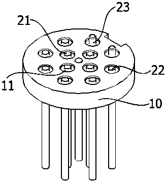
The number of pins included in the traditional base is generally 7~8, and the pins are arranged along the outer edge of the base, and the middle area formed by the pins is used for mounting chips. However, for optical sub-modules with more pins , for example, for optical communication products with more than 10 pins, the base cannot leave enough space to install electronic devices such as chips

Method used


Image

  • Optical secondary module and light module
  • Optical secondary module and light module
  • Optical secondary module and light module

Examples


Embodiment Construction

[0018] In order to make the object, technical solution and advantages of the present invention clearer, the present invention will be further described in detail below in conjunction with the accompanying drawings. Obviously, the described embodiments are only some embodiments of the present invention, rather than all embodiments . Based on the embodiments of the present invention, all other embodiments obtained by persons of ordinary skill in the art without making creative efforts belong to the protection scope of the present invention.

[0019] As mentioned above, the base of the coaxial package of the traditional optical sub-module generally contains 7 to 8 pins. When the number of pins exceeds a certain number (such as 10), most of the space on the base will be occupied. The pins are occupied, so that no space can be reserved for the installation of optical communication electronic devices. Especially for optical communication products with high transmission rate, there ...


PUM


Abstract

The invention provides an optical secondary module. The module comprises a base, an insulation plate and a first pin which penetrates through the base and is used for signal transmission, the first pin is located in a projection area of the insulation plate on the base, and an electric conduction access is formed in the surface, facing the base, of the insulation plate; one end of the electric conduction access is electrically connected with the first pin, and the other end of the electric conduction access is electrically connected with a chip arranged on the insulation plate. The first pin located in the projection area of the insulation plate on the base is connected with the electric conduction access in the insulation plate, the first pin is electrically with the chip through the electric conduction access, so that signal transmission is achieved, and therefore the mounting space occupied by the additionally-arranged pin on the base is provided for the chip through the insulationplate; electric communication connection between the pin and the chip is achieved through the electric conduction access arranged on the insulation plate, and on the premise of meeting the requirementof additionally arranging pin on the optical secondary module, the mounting space of electronic devices such as chips on the optical secondary module can be guaranteed.

Description

technical field [0001] The invention relates to the technical field of optical communication, in particular to an optical module and an optical module. Background technique [0002] There are two main packaging technologies used in optical communication products such as optical sub-modules, one is COB (Chip-on-Borad) packaging technology, that is, chip-on-board packaging; the other is TO (Transistor-Outline) packaging technology, That is, the coaxial TO package. Because the coaxial TO package has many advantages such as simple packaging, good versatility, and fast production efficiency, it is widely used in optical communication products. [0003] At present, the base of the coaxial package generally includes a base body and pins provided on the base body, and the top surface of the base body is used for mounting optical communication devices such as optoelectronic chips. With the continuous improvement of the transmission rate of optical communication products, in order t...

Claims


Application Information

Patent Timeline
IPC IPC(8): G02B6/42
CPCG02B6/4274
Inventor 王永强
Owner HISENSE BROADBAND MULTIMEDIA TECH
Learn More