
Pixel array substrate

A pixel array substrate and pixel electrode technology, which is applied in the field of array substrates, can solve problems such as display panel bubbles, display panel defects, and color filter patterns that are easy to form sunken areas, and achieve the effect of reducing the probability of bubbles

Active Publication Date: 2020-12-04
AU OPTRONICS CORP
View PDF12 Cites 0 Cited by
  • Summary
  • Abstract
  • Description
  • Claims
  • Application Information

AI Technical Summary

Problems solved by technology

[0003] However, the active element layer has different element densities in different areas, so when multiple color filter patterns of the color filter layer are formed in areas with low element density, a sunken area is easily formed between two adjacent color filter patterns.
When the color filter layer with the sunken area is combined with the display medium and the second substrate to form a display panel, the display panel is prone to bubbles caused by the sunken area, resulting in defective display panels.

Method used


Image

  • Pixel array substrate
  • Pixel array substrate
  • Pixel array substrate

Examples


Embodiment Construction

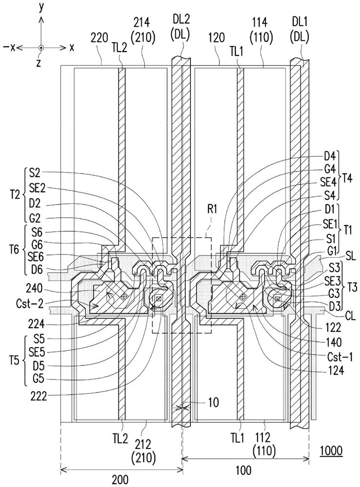
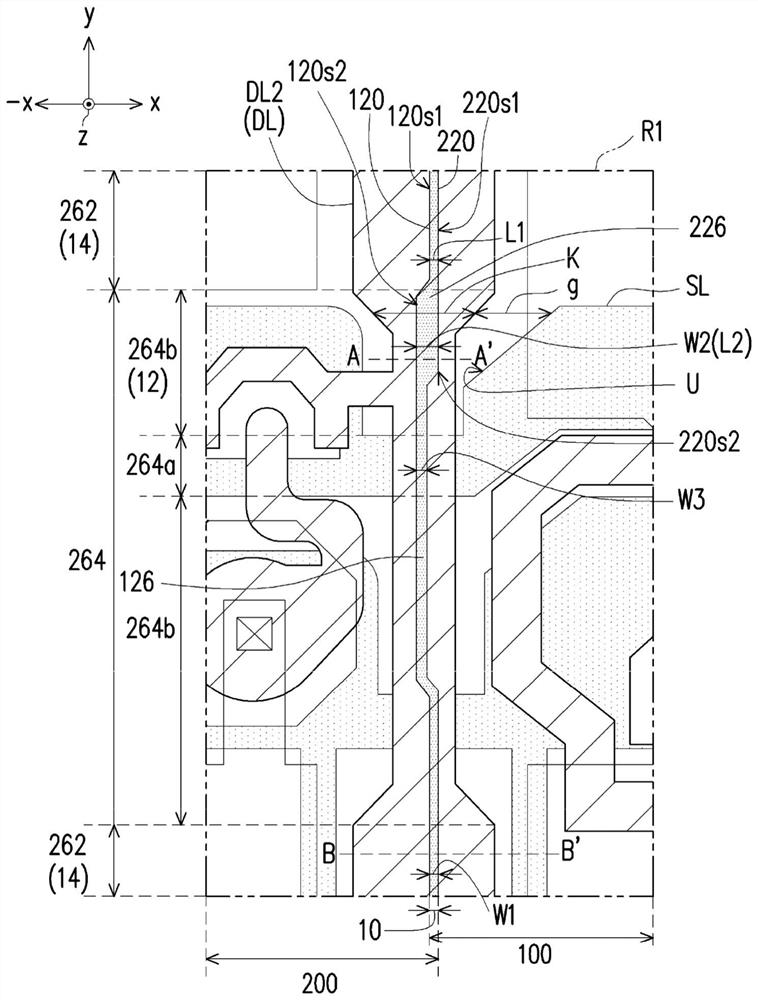
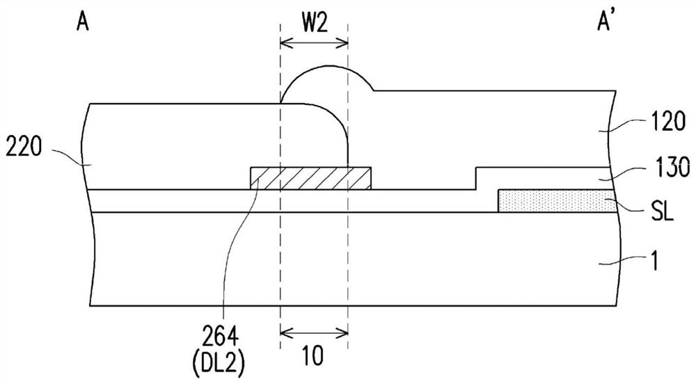
[0069] figure 1 It is a top view of a pixel array substrate according to an embodiment of the present invention. figure 2 for figure 1 The enlarged schematic diagram of the partial R1 of the pixel array substrate. image 3 based on figure 2 The schematic cross-sectional view of the pixel array substrate drawn by the section line A-A'. Figure 4 based on figure 2 The schematic cross-sectional view of the pixel array substrate drawn by the section line B-B'.

[0070] Please refer to figure 1 , figure 2 , image 3 and Figure 4 , the pixel array substrate 1000 includes a substrate 1 (drawn in image 3 and Figure 4 ) and a plurality of first pixel units 100 , a plurality of second pixel units 200 , a plurality of scan lines SL and a plurality of data lines DL disposed on the substrate 1 . The data lines DL and the scan lines SL are arranged alternately. figure 1 Draw a first pixel unit 100, a second pixel unit 200, a scan line SL and two data lines DL1, DL2 as an ...


PUM


Abstract

A pixel array substrate including a first pixel unit, a second pixel unit adjacent to the first pixel unit, a scan line electrically connected to at least one of a first thin film transistor of the first pixel unit and a second thin film transistor of the second pixel unit and a data line electrically connected to at least one of the first thin film transistor of the first pixel unit and the second thin film transistor of the second pixel unit and crossed the scan line is provided. A first color filter of the first pixel unit and a second color filter of the second pixel unit are partially overlapped to form a stacking region of the first color filter and the second color filter. The data line has a wide portion and a narrow portion. A width of a portion of the stacking region on the narrow portion of the date line is larger than a width of a portion of the stacking region on the wide portion of the date line.

Description

technical field [0001] The present invention relates to an array substrate, and in particular to a pixel array substrate. Background technique [0002] The display panel includes a first substrate, an active element layer disposed on the first substrate, a second substrate disposed opposite to the first substrate, and a display medium disposed between the first substrate and the second substrate. Generally speaking, if the display medium is a non-self-luminous material (such as liquid crystal), the display panel further includes a color filter layer disposed on the second substrate, so that the display panel can display color images. In the process of the display panel, the first substrate with the active device layer and the second substrate with the color filter layer are assembled. When the assembly accuracy of the two is not good, the display quality will be reduced. In view of this, the color filter layer can be directly fabricated on the first substrate having the pix...

Claims


Application Information

Patent Timeline
Patent Type & Authority Patents(China)
IPC IPC(8): G02F1/1335G02F1/1362H01L27/12
CPCG02F1/133514G02F1/136209G02F1/136286G02F1/136222H01L27/124
Inventor 纪志贤曾胜煊黄圣硕李美慧王世杰刘昌宗庄凯钧黄以钧郑世彬
Owner AU OPTRONICS CORP
Learn More