Method for designing fully randomized silicon-based waveguide optical grating on basis of chaotic particle swarm optimization algorithm

A technology of chaotic particle swarms and waveguide gratings, applied in optical waveguides, optics, light guides, etc., can solve the problems of complex manufacturing process of silicon-based devices, difficult for designers to control, and many design parameters. Strong, improve work efficiency

Inactive Publication Date: 2018-06-29
SHANDONG UNIV
View PDF1 Cites 6 Cited by
  • Summary
  • Abstract
  • Description
  • Claims
  • Application Information

AI Technical Summary

Problems solved by technology

[0005] The design parameters of the grating directly affect the coupling performance of the grating involved. For a grating coupler with a general uniform structure, there are fewer design parameters, which also leads to a low coupling efficiency, usually not more than 30%, bu...

Method used


Image

  • Method for designing fully randomized silicon-based waveguide optical grating on basis of chaotic particle swarm optimization algorithm
  • Method for designing fully randomized silicon-based waveguide optical grating on basis of chaotic particle swarm optimization algorithm
  • Method for designing fully randomized silicon-based waveguide optical grating on basis of chaotic particle swarm optimization algorithm

Examples


Embodiment Construction

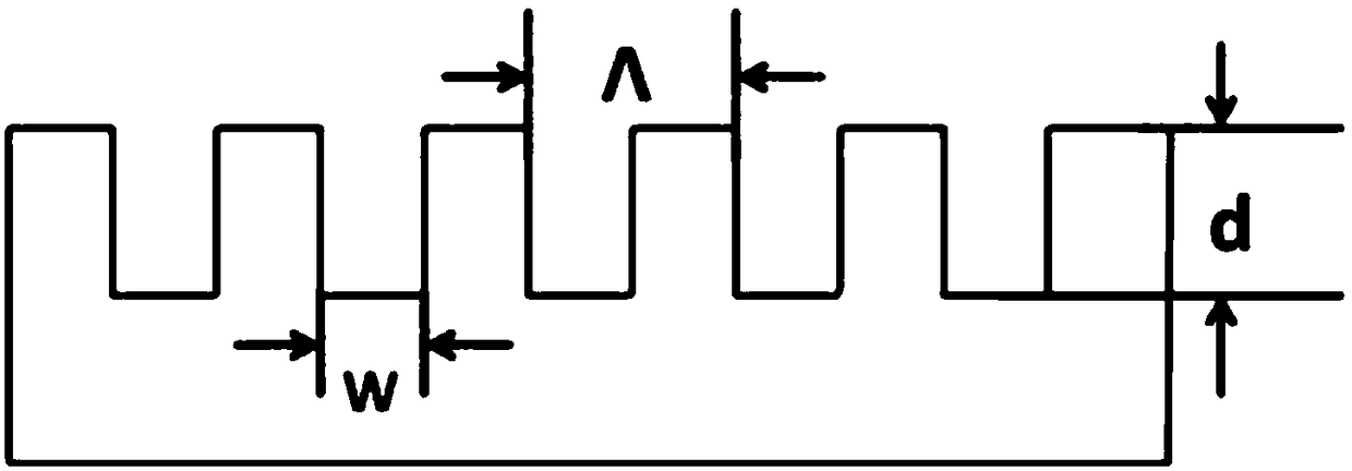
[0019] The design method of the all-random silicon-based waveguide grating based on the chaotic particle swarm algorithm of the present invention can effectively and rapidly design the all-random grating.

[0020] Depend on figure 1 Given the basic structure of the grating, it can be seen that the design parameters of the uniform grating mainly include the etching depth d, the period Λ and the duty cycle w / Λ, the light source is input from the single-mode fiber to the grating area of ​​the grating coupler, and through the grating area The coupling effect couples the incident light into the waveguide region of the waveguide layer. To combine the incident light into the waveguide, the grating period needs to be designed so that it meets the phase matching condition:

[0021]

[0022] In the formula, β is the propagation constant of the silicon waveguide, m is the diffraction order, and the maximum order of the main diffraction pole is -1, k 0 Indicates the reflection coupli...


PUM


Abstract

The invention relates to a method for designing a fully randomized silicon-based waveguide optical grating on the basis of a chaotic particle swarm optimization algorithm. Uniform optical grating design parameters are made inhomogeneous, the overall variation of the optical grating is designed as the change of each periodic block, and a coupling efficiency value under the case of each parameter isan adaptation degree in the particle swarm optimization algorithm; when a particle swarm evolves to the next generation, each particle updates itself by tracking two optimal solutions including pbestand gbest; when a boundary position value is taken as a particle value, chaotic variable processing is conducted, and a global search function is achieved; an initial value is provided for a chaoticvariable, and a group of random sequences with ergodicity and pseudo-randomness are generated through iteration of a chaotic iterative equation; a coupling efficiency standard required for the opticalgrating is set, when a particle swarm optimization result reaches the required standard, the process stops automatically, and the particle value corresponding to the adaptation degree is the demandeddesign parameter value. Systematic design of the fully randomized optical grating is achieved, and design parameters and the coupling efficiency of the optical grating can be effectively and quicklyobtained.

Description

technical field [0001] The invention relates to a design method for a silicon-based waveguide grating coupling device, belonging to the technical field of photonic devices. Background technique [0002] Integrated optical components integrate conventional discrete optical components with various functions onto the surface of the same optical substrate, and have the same function as a large optical system composed of multiple discrete optical components to process optical signals. Compared with conventional optical components, integrated optical components have the advantages of small size, light weight, low power consumption, high reliability, and long life. At present, integrated optical components have played a very important role in communication, military, electric power, astronomy, sensing and other application fields. Especially in the application in the military field, it has the incomparable superiority of the conventional optical system. [0003] Optical waveguide...

Claims


Application Information

Patent Timeline
IPC IPC(8): G02B27/00G02B6/12
CPCG02B27/0012G02B6/12009
Inventor 赵佳赵昊
Owner SHANDONG UNIV
Why Eureka
Try Eureka