
coa array substrate

A technology for array substrates and substrate substrates, applied in instruments, nonlinear optics, optics, etc., can solve problems such as uncontrollable electrical signals of pixel electrodes 410, inability to remove metal oxides by etching, incomplete removal of exposure, etc., to reduce Metal oxide residues, avoiding uncontrollable electrical signals, and reducing the effect of terrain differences

Active Publication Date: 2020-07-28
SHENZHEN CHINA STAR OPTOELECTRONICS SEMICON DISPLAY TECH CO LTD
View PDF5 Cites 0 Cited by
  • Summary
  • Abstract
  • Description
  • Claims
  • Application Information

AI Technical Summary

Problems solved by technology

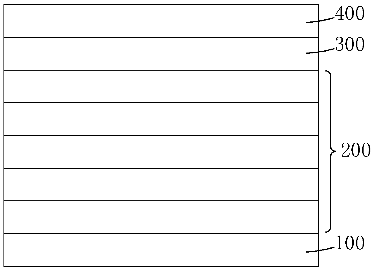
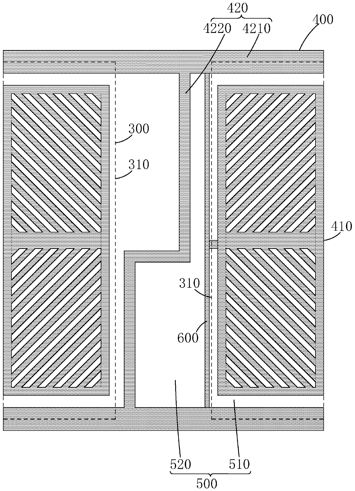
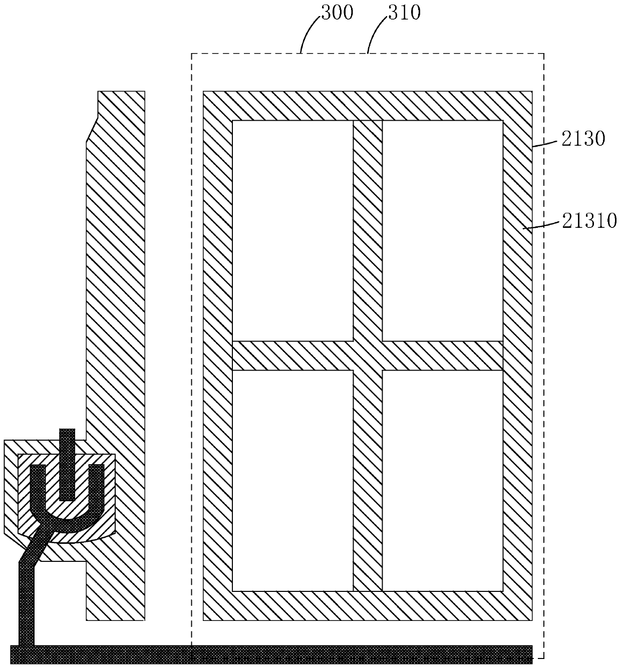
[0008] The color color resist layer 300 includes several color resist units 310 arranged at intervals, the several color resist units 310 respectively correspond to the several pixel electrodes 410 up and down, and the outer edges of the several color resist units 310 respectively exceed For the outer edges of the plurality of pixel electrodes 410, since the color-resist unit 310 is thicker, a relatively large topographical level difference is likely to appear on the COA-type array substrate corresponding to the outer edge of the color-resist unit 310. When the transparent conductive layer 400 made of metal oxide material is formed on the color resist layer 300, the photoresist is easily deposited at the position corresponding to the outer edge of the color resist unit 310 to form a thick film, which cannot be removed after exposure and development (ie, exposure Incomplete), the metal oxide under the photoresist cannot be removed by etching, and finally a metal oxide residual line 600 appears on the side of the pixel electrode 410. When the metal oxide residual line 600 connects the pixel electrode 410 and When the horizontal electrode 4210 in the first light-shielding common electrode 420 is used, the electrical signal of the pixel electrode 410 cannot be controlled.

Method used


Image

  • coa array substrate
  • coa array substrate
  • coa array substrate

Examples


Embodiment Construction

[0039] In order to further illustrate the technical means adopted by the present invention and its effects, the following describes in detail in conjunction with preferred embodiments of the present invention and accompanying drawings.

[0040] see Figure 4 to Figure 9 , the present invention provides a COA type array substrate, comprising a base substrate 10, a TFT layer 20 disposed on the base substrate 10, a color color resist layer 30 disposed on the TFT layer 20, a color resist layer 30 disposed on the A transparent conductive layer 40 on the color resist layer 30;

[0041] The transparent conductive layer 40 includes several pixel electrodes 41 arranged at intervals and arranged in an array, and a first light-shielding common electrode 42 located in the interval region 50 of the several pixel electrodes 41 and not connected to the several pixel electrodes 41 ;

[0042] The color resistance layer 30 includes a plurality of color resistance units 31 arranged at interval...


PUM

PropertyMeasurementUnit
thicknessaaaaaaaaaa
thicknessaaaaaaaaaa
thicknessaaaaaaaaaa

Abstract

A COA array substrate. By providing all or part of an outer edge of a color resist unit (31) on a first metal layer (21) and / or a second metal layer (24), the difference in topographic sections of the COA array substrate at the outer edge of the color resist unit (31) can be reduced by means of the padding effect of the first metal layer (21) and / or the second metal layer (24), so that the thickness of a photoresist with which the outer edge of the color resist unit (31) is coated can be reduced when a transparent conductive layer (40) is patterned, thereby easily removing the photoresist by means of exposure and development. In addition, the first metal layer (21) and the second metal layer (24) have reflective characteristics, which can improve the exposure effect, so that the photoresist with which the outer edge of the color resist unit (31) is coated is fully exposed and removed by means of development. The COA array substrate eliminates or reduces the metal oxide residual at the outer edge of the color resist unit (31), which avoids the out-of-control situations of an electrical signal of a pixel electrode (41).

Description

technical field [0001] The present invention relates to the field of display technology, in particular to a COA type array substrate. Background technique [0002] Liquid crystal display (Liquid Crystal Display, LCD) has many advantages such as thin body, power saving, and no radiation, and has been widely used, such as: mobile phones, personal digital assistants (PDA), digital cameras, computer screens and notebook computers screen etc. [0003] Most of the liquid crystal display devices currently on the market are backlight liquid crystal display devices, which include a housing, a liquid crystal panel disposed in the housing, and a backlight module disposed in the housing. The structure of a traditional liquid crystal panel is composed of a color filter substrate (Color Filter), a thin film transistor array substrate (Thin Film TransistorArray Substrate, TFT Array Substrate), and a liquid crystal layer (Liquid Crystal Layer) arranged between the two substrates. , its wo...

Claims


Application Information

Patent Timeline
Patent Type & Authority Patents(China)
IPC IPC(8): G02F1/1362
CPCG02F1/1362G02F1/136222
Inventor 曹武
Owner SHENZHEN CHINA STAR OPTOELECTRONICS SEMICON DISPLAY TECH CO LTD
Learn More