Semiconductor structures and methods of forming them

A semiconductor and patterning technology, which is applied in the direction of semiconductor devices, semiconductor/solid-state device manufacturing, electrical components, etc., can solve the problems of low yield rate and many defects, and achieve the effect of improving yield rate, reducing the generation of defects, and reducing the impact

Active Publication Date: 2020-07-10
SEMICON MFG INT (SHANGHAI) CORP +1
View PDF3 Cites 0 Cited by
  • Summary
  • Abstract
  • Description
  • Claims
  • Application Information

AI Technical Summary

Problems solved by technology

[0005] However, in the existing technology, the introduction of "high-K metal gate" semiconductor structure often has the problem of many defects and low yield

Method used


Image

  • Semiconductor structures and methods of forming them
  • Semiconductor structures and methods of forming them
  • Semiconductor structures and methods of forming them

Examples


Embodiment Construction

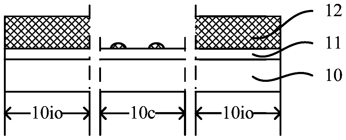
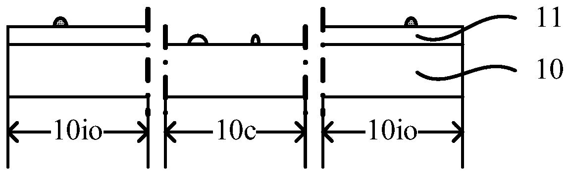
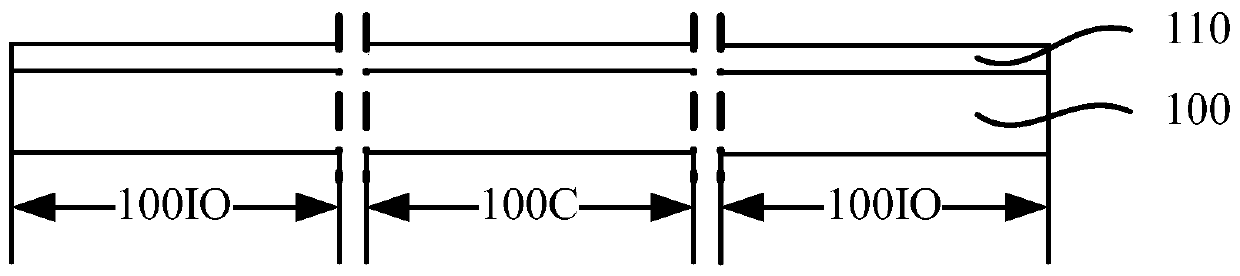
[0034] It can be seen from the background art that in the prior art, the semiconductor structure with the introduction of "high-K metal gate" often has the problems of many defects and low yield. Combining with a method of forming a semiconductor structure with a "high-K metal gate", the reason for the problem of many defects and low yield is analyzed:

[0035] Semiconductor devices are mainly divided into core (Core) devices and input and output (Input and Output, IO) devices according to their functions. In order to reduce the size of the semiconductor device and improve the integration of the semiconductor device, the size of the core device is smaller than the size of the input and output devices.

[0036] In addition, the operating voltage of the input and output devices is much higher than that of the core device to obtain stronger driving capability. In order to prevent problems such as electrical breakdown, when the operating voltage of the device is higher, the thick...


PUM


Abstract

The invention relates to a semiconductor structure and a formation method thereof. The method comprises that a substrate is provided; an oxide layer is formed on the substrate; oxidation treatment iscarried out on the surface of the oxide layer; and the oxide layer after oxidation treatment is patterned to remove part of the oxide layer. According to technical schemes of the invention, the oxidation treatment is carried out on the surface of the oxide layer after formation of the oxide layer, so that residues in the surface of the oxide layer is removed, influence of the residues on subsequent technologies is reduced, defects generated in the oxide layer patterning process is reduced, and the yield rate of the semiconductor structure is improved.

Description

technical field [0001] The invention relates to the field of semiconductor manufacturing, in particular to a semiconductor structure and a forming method thereof. Background technique [0002] With the continuous development of integrated circuit manufacturing technology, semiconductor devices are developing towards higher component density and higher integration. The geometric dimensions of semiconductor devices continue to shrink following Moore's Law. As the most basic semiconductor device, the size of the transistor decreases as the size of the semiconductor device decreases. [0003] When the size of semiconductor devices is reduced to a certain extent, various secondary effects caused by the physical limits of semiconductor devices appear one after another, and it becomes more and more difficult to scale down the feature size of semiconductor devices. Among them, for transistors, the reduction of size will cause many problems such as increase of leakage current and d...

Claims


Application Information

Patent Timeline
Patent Type & Authority Patents(China)
IPC IPC(8): H01L21/28H01L29/51
CPCH01L21/28158H01L21/28185H01L21/28211H01L29/51
Inventor 杨志勇刘焕新
Owner SEMICON MFG INT (SHANGHAI) CORP
Why Eureka
Try Eureka