Conductive pattern printing and linear scanning solidification integrated system and method
A conductive pattern, linear scanning technology, used in printing devices, printing, typewriters, etc., can solve the problems of slow curing, uneven curing, and uneven surface drying of conductive ink, so as to reduce penetration, increase curing area, reduce The effect of contact time
- Summary
- Abstract
- Description
- Claims
- Application Information
AI Technical Summary
Problems solved by technology
Method used
Image
Examples
Embodiment Construction
[0042] In order to make the object, technical solution and advantages of the present invention more clear, the present invention will be further described in detail below in conjunction with the examples. It should be understood that the specific embodiments described here are only used to explain the present invention, not to limit the present invention.
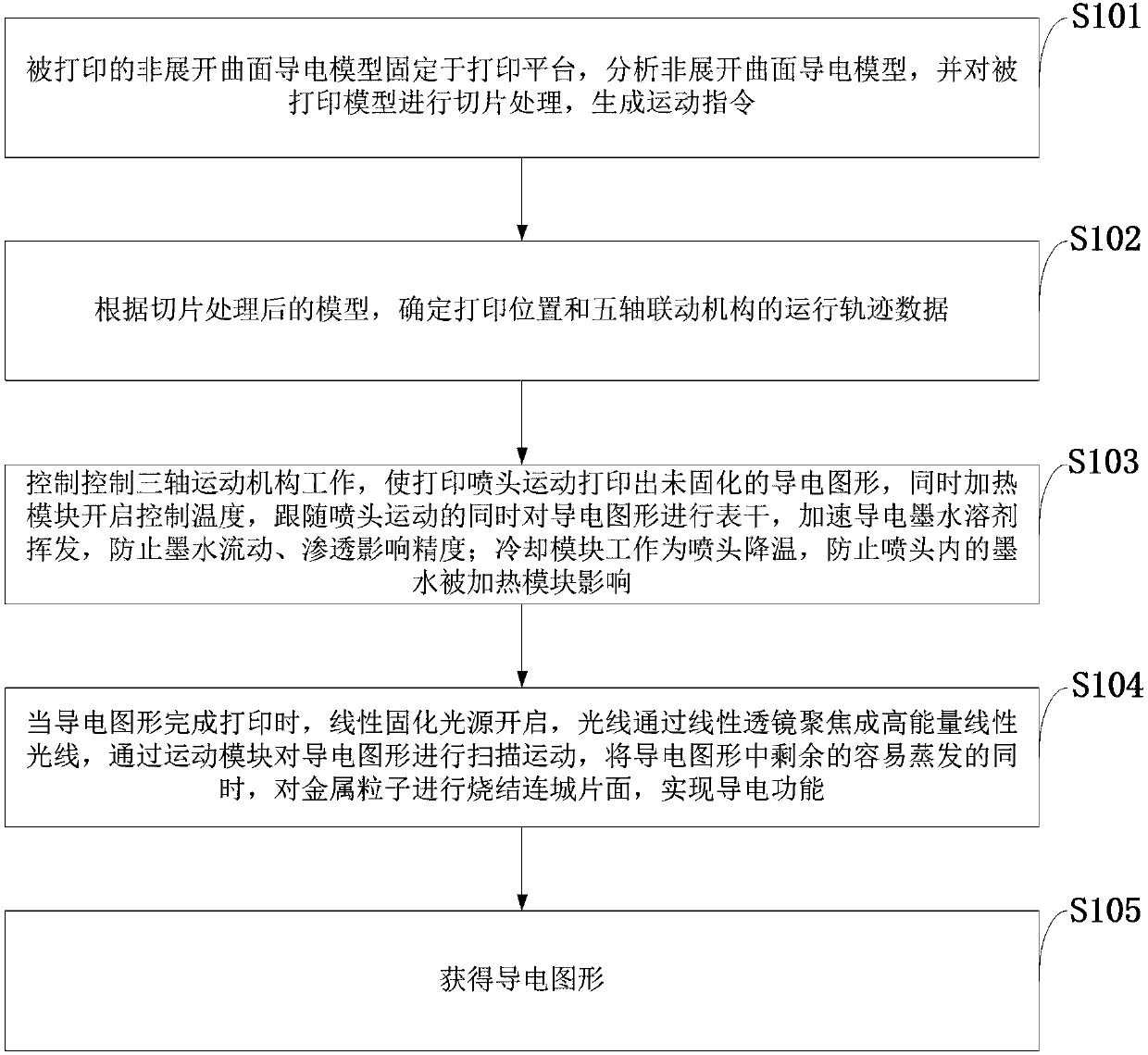
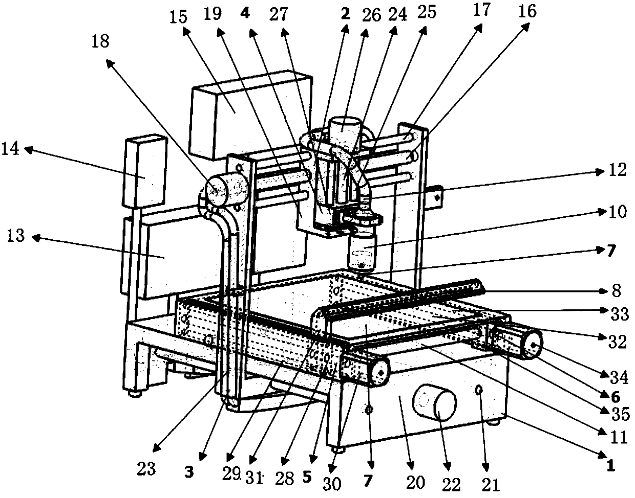
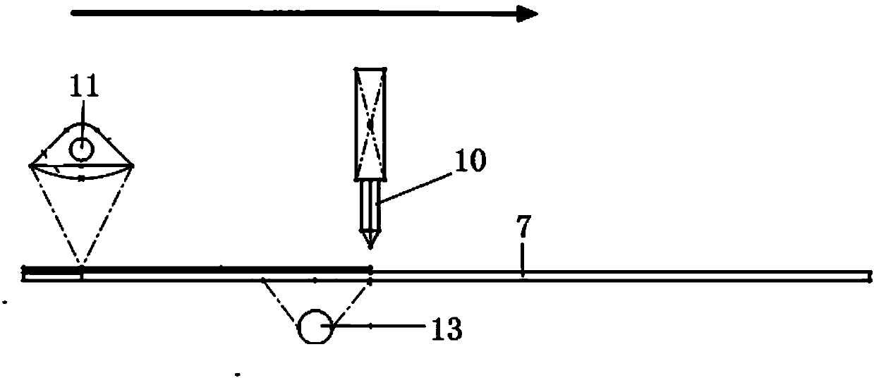
[0043] The invention uses a multi-axis motion mechanism to print conductive ink on the non-expanded curved surface, and at the same time, the heating rod under the printing platform moves with the printing nozzle to accelerate solvent volatilization. After printing, the conductive ink of the linear light source is cured with photons, and finally an electronic circuit is formed. ;It can effectively solve the problems of slow curing of conductive ink during printing, uneven border caused by ink dripping, uneven surface dryness, uneven curing, etc., effectively improves printing efficiency and improves the quality of printed it...
PUM
 Abstract
Description
Claims
Application Information
 - Generate Ideas
- Intellectual Property
- Life Sciences
- Materials
- Tech Scout
- Unparalleled Data Quality
- Higher Quality Content
- 60% Fewer Hallucinations
Browse by: Latest US Patents, China's latest patents, Technical Efficacy Thesaurus, Application Domain, Technology Topic, Popular Technical Reports.
© 2025 PatSnap. All rights reserved.Legal|Privacy policy|Modern Slavery Act Transparency Statement|Sitemap|About US| Contact US: help@patsnap.com


