Manufacturing method of touch sensing layer, display screen and display

A touch sensing and manufacturing method technology is applied to the manufacturing field of display screens, displays, and touch sensing layers, which can solve the problems of increased process cost and unfavorable release of production capacity of exposure machines, so as to reduce process costs, release production capacity, and simplify processes Effect

Active Publication Date: 2021-09-28
WUHAN CHINA STAR OPTOELECTRONICS SEMICON DISPLAY TECH CO LTD
View PDF2 Cites 0 Cited by
  • Summary
  • Abstract
  • Description
  • Claims
  • Application Information

AI Technical Summary

Problems solved by technology

This method uses more masks and requires multiple exposures, which is not conducive to the release of the exposure machine's capacity, resulting in increased process costs

Method used


Image

  • Manufacturing method of touch sensing layer, display screen and display
  • Manufacturing method of touch sensing layer, display screen and display
  • Manufacturing method of touch sensing layer, display screen and display

Examples


Embodiment Construction

[0029] The following will clearly and completely describe the technical solutions in the embodiments of the present invention with reference to the drawings in the embodiments of the present invention. Apparently, the described embodiments are some, not all, embodiments of the present invention. Based on the embodiments of the present invention, all other embodiments obtained by persons of ordinary skill in the art without making creative efforts shall fall within the protection scope of the present invention.

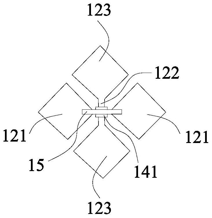
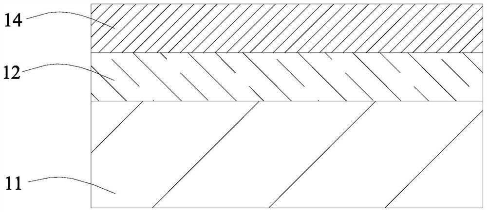
[0030] An embodiment of the present invention provides a method for manufacturing a touch sensing layer, which is used for manufacturing the touch sensing layer. The touch sensing layer may be composed of a plurality of film layers, and the touch sensing layer composed of a plurality of film layers may include a plurality of emitting electrodes Tx and a plurality of receiving electrodes Rx arranged regularly. For example, the touch sensing layer may include a pluralit...


PUM


Abstract

The invention provides a manufacturing method of a touch sensing layer, a display screen and a display. The display screen is made by the manufacturing method, and the display screen includes the display screen. The solution of the present invention only needs one mask plate and one exposure process to manufacture the insulator pattern and the electrode pattern in the touch sensing layer of the display screen. Compared with the existing technology, the process can be simplified, the production capacity of the exposure machine can be released, and the process cost can be reduced.

Description

technical field [0001] The invention relates to the field of display technology, in particular to a method for manufacturing a touch sensing layer, a display screen and a display. Background technique [0002] The touch display screen includes a touch sensor layer (Touch Sensor), which is a device for realizing touch sensing. The touch sensing layer generally includes a substrate on which electrodes, insulators, metal bridges, and packaging layers are sequentially formed. The manufacturing process of the touch sensing layer uses a photolithography process, wherein the formation of electrodes and insulators requires a photolithography process respectively, that is, providing two masks and using the two masks to form patterns of electrodes and insulators. This method uses more masks and requires multiple exposures, which is not conducive to the release of the production capacity of the exposure machine, resulting in increased process costs. Contents of the invention [000...

Claims


Application Information

Patent Timeline
Patent Type & Authority Patents(China)
IPC IPC(8): H01L27/32G03F7/20G06F3/041
CPCG03F7/2022G06F3/041H10K59/40
Inventor 胡重粮
Owner WUHAN CHINA STAR OPTOELECTRONICS SEMICON DISPLAY TECH CO LTD
Why Eureka
Try Eureka