A kind of array substrate and display device

A technology for array substrates and carrier substrates, applied in instruments, acquisition/arrangement of fingerprints/palmprints, electric solid-state devices, etc., can solve problems such as poor sensitivity, and achieve the effect of improving acquisition sensitivity and improving sensitivity

Active Publication Date: 2020-11-13
SHANGHAI AVIC OPTOELECTRONICS
View PDF4 Cites 0 Cited by
  • Summary
  • Abstract
  • Description
  • Claims
  • Application Information

AI Technical Summary

Problems solved by technology

Existing optical display devices for fingerprint collection generally integrate photodiodes in the display device for information collection, but the sensitivity of the existing display devices for fingerprint collection is relatively poor

Method used


Image

  • A kind of array substrate and display device
  • A kind of array substrate and display device
  • A kind of array substrate and display device

Examples


Embodiment Construction

[0023] The following will clearly and completely describe the technical solutions in the embodiments of the present invention with reference to the accompanying drawings in the embodiments of the present invention. Obviously, the described embodiments are only some, not all, embodiments of the present invention. Based on the embodiments of the present invention, all other embodiments obtained by persons of ordinary skill in the art without making creative efforts belong to the protection scope of the present invention.

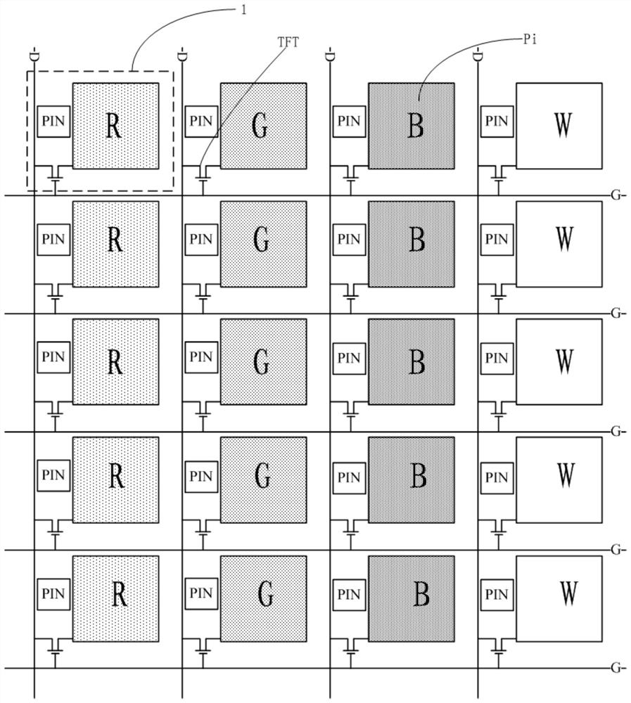
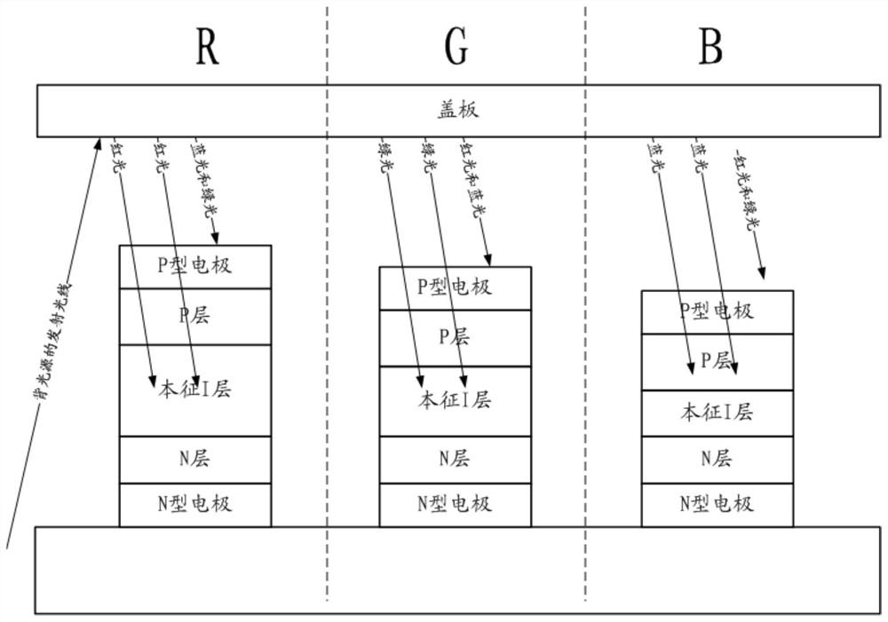
[0024] As mentioned in the background, with the development of electronic science and technology, many display devices such as smart phones and tablet computers begin to have a fingerprint identification function. The main implementation methods of fingerprint recognition technology are optical, capacitive and so on. Among them, the fingerprint identification technology that adopts optical fingerprint collection has a relatively large identification range and ...


PUM

PropertyMeasurementUnit
thicknessaaaaaaaaaa
thicknessaaaaaaaaaa
thicknessaaaaaaaaaa

Abstract

The invention discloses an array substrate and a display device. The array substrate includes: a sub-pixel array composed of sub-pixels, the sub-pixels include colored sub-pixels, and the colored sub-pixels include red sub-pixels, green sub-pixels and blue sub-pixels; The region corresponding to at least one colored sub-pixel is respectively provided with at least one photodiode, and the thickness of the intrinsic I layer of the photodiode is a thickness that only responds to the color of the corresponding colored sub-pixel. It can be seen from the above that in the technical solution provided by the present invention, the photodiode is arranged in the corresponding area of ​​the colored sub-pixel, and the thickness of the intrinsic I layer of the photodiode is the thickness that only responds to the color of the corresponding colored sub-pixel. The thickness of the intrinsic I layer of the photodiode is matched with the color of the corresponding colored sub-pixel to avoid interference of other color lights to the photodiode, improve the collection sensitivity of the photodiode, and then improve the sensitivity of the display device.

Description

technical field [0001] The present invention relates to the field of display technology, and more specifically, to an array substrate and a display device. Background technique [0002] With the development of electronic science and technology, many display devices such as smart phones and tablet computers begin to have a fingerprint identification function. The main implementation methods of fingerprint recognition technology are optical, capacitive and so on. Among them, the fingerprint identification technology that adopts optical fingerprint collection has a relatively large identification range and relatively low cost. Existing optical fingerprint collection display devices generally integrate photodiodes in the display device for information collection. However, the existing display devices have poor sensitivity when collecting fingerprints. Contents of the invention [0003] In view of this, the present invention provides an array substrate and a display device, w...

Claims


Application Information

Patent Timeline
Patent Type & Authority Patents(China)
IPC IPC(8): H01L27/12G06K9/00
CPCH01L27/1214G06V40/1318
Inventor 蔡敏秦丹丹时成瑛秦锋夏志强刘金娥
Owner SHANGHAI AVIC OPTOELECTRONICS
Why Eureka
Try Eureka