A coupled inductor boost inverter and its control method

A technology of coupled inductors and control methods, which is applied to electrical components, high-efficiency power electronic conversion, and conversion of AC power input to DC power output. It can solve problems such as low boost ratio, achieve improved conversion efficiency, increase boost ratio, Effect of Reducing Switching Loss

Inactive Publication Date: 2020-05-12
HOHAI UNIV WENTIAN COLLEGE
View PDF3 Cites 0 Cited by
  • Summary
  • Abstract
  • Description
  • Claims
  • Application Information

AI Technical Summary

Problems solved by technology

[0006] Aiming at the problem of low boost ratio in the boost inverter in the prior art, the present invention provides a coupled inductor boost inverter and its control method

Method used


Image

  • A coupled inductor boost inverter and its control method
  • A coupled inductor boost inverter and its control method
  • A coupled inductor boost inverter and its control method

Examples


Embodiment 1

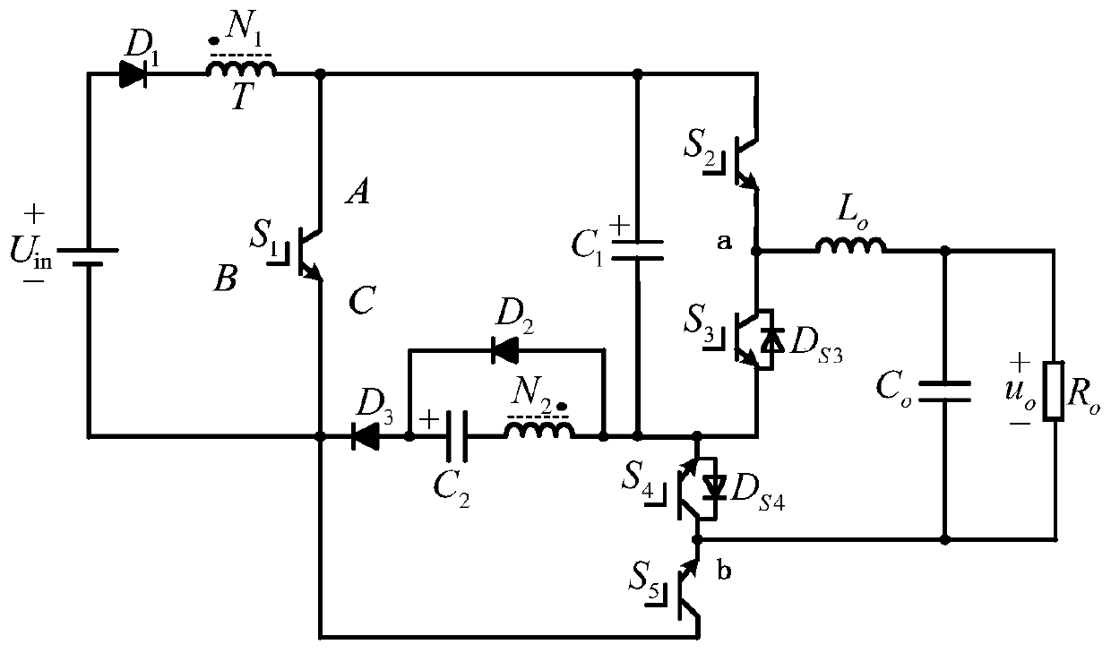
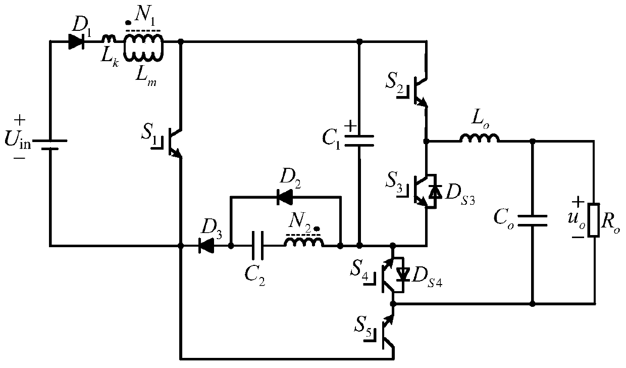
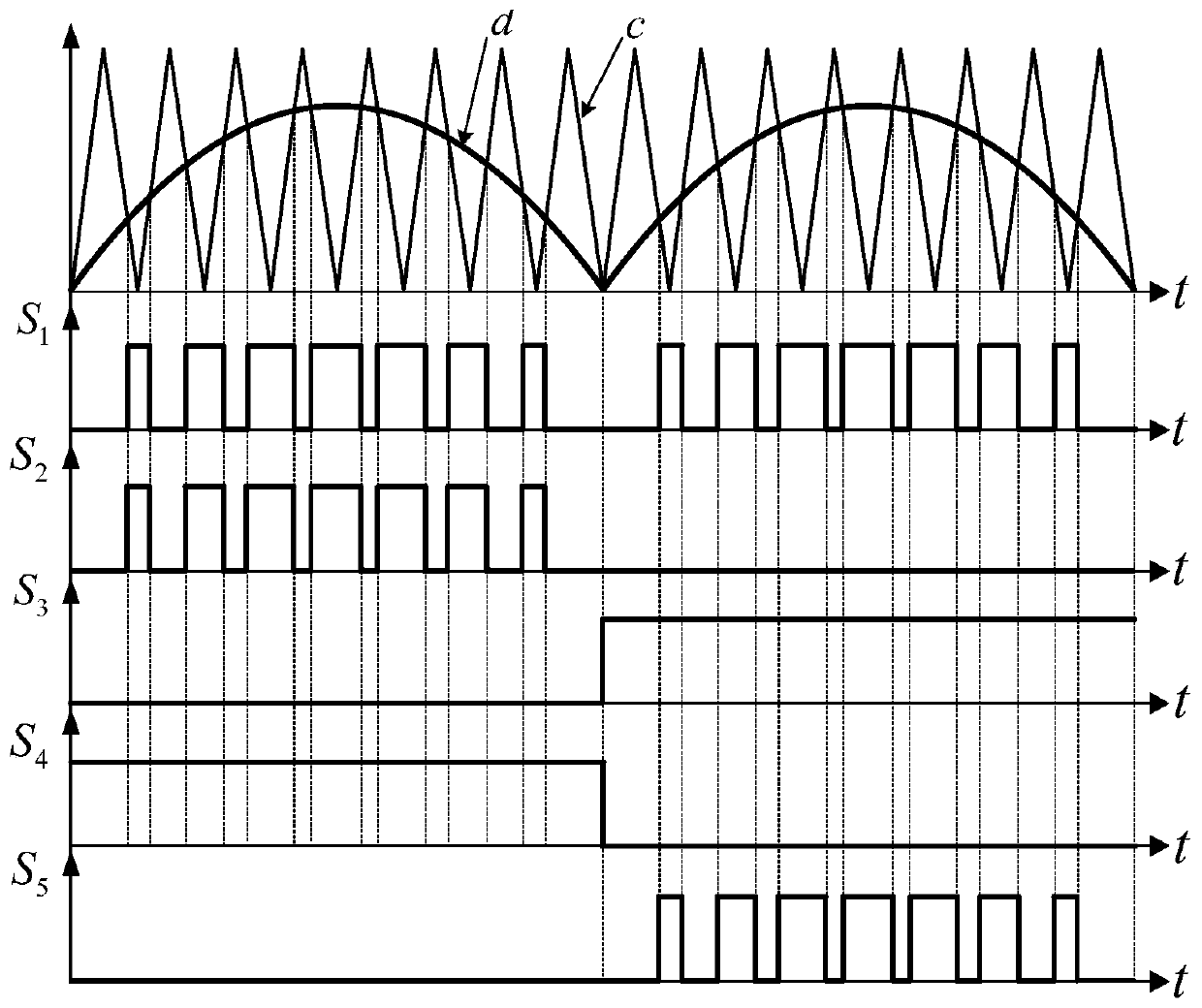
[0058] Such as figure 1 As shown, a coupled inductor boost inverter in this embodiment includes a diode D 1 、D 2 、D S3 and D S4 , switch tube S 1 , S 2 , S 3 , S 4 and S 5 ; The primary winding N of the coupled inductor T 1 and the secondary winding N 2 ; Capacitance C 1 ;

[0059] Diode D 1 The anode is connected to the input power supply U in One end, the diode D 1 The cathode is connected to the primary winding N of the coupled inductor T 1 end of the same name;

[0060] Primary winding N of coupled inductor T 1 Non-identical terminal and switch tube S 1 Terminal A, switch tube S 2 A terminal and capacitor C 1 connected at one end;

[0061] Switch tube S 1 C terminal, diode D 3 Cathode, switch tube S 5 A terminal and input power U in The other end is connected;

[0062] Diode D 3 anode, diode D 2 Cathode and Capacitor C 2 connected at one end;

[0063] Capacitance C 2 The other end and the primary winding N of the coupled inductor T 2 Non-iden...

Embodiment 2

[0072] to combine figure 1 , a coupled inductor boost inverter of this embodiment is further improved on the basis of Embodiment 1, because the capacitor C 1 and C 2 Both are intermediate energy storage elements, which play the role of energy conversion, and the capacitor C 1 and C 2 All are non-polar capacitors, which make the circuit work reliably and increase the working life of the circuit.

Embodiment 3

[0074] to combine figure 1 , a coupled inductance boost inverter of this embodiment is further improved on the basis of embodiment 1 or 2, and further includes a filter, the nodes a and b are connected to the input ends of the filter, and the filter The output terminal is connected to the load R o or the grid.

[0075] In this embodiment, the step-up inverter is completed, and the output terminal of the filter, that is, the output voltage u o directly for the load R o power supply, or the output voltage u o Feedback to the grid.


PUM


Abstract

The invention discloses a coupled inductance step-up inverter and a control method thereof, belonging to the technical field of power electronic converters. It includes diode D 1 、D 2 、D S3 and D S4 , switch tube S 1 , S 2 , S 3 , S 4 and S 5 ; The primary winding N of the coupled inductor T 1 and the secondary winding N 2 ; Capacitance C 1 ; Diode D 1 The anode is connected to the input power supply U in One end, the diode D 1 The cathode is connected to the primary winding N of the coupled inductor T 1 Terminal of the same name; primary winding N of coupled inductor T 1 Non-identical end and switch tube S 1 Terminal A, switch tube S 2 A terminal and capacitor C 1 Connected at one end; switch tube S 1 C terminal, diode D 3 Cathode, switch tube S 5 A terminal and input power U in The other end is connected; diode D 3 anode, diode D 2 Cathode and Capacitor C 2 connected at one end. Aiming at the problem of low boost ratio in the prior art boost inverter, it has high integration, high boost ratio and more flexible regulation of boost ratio.

Description

technical field [0001] The invention relates to the technical field of power electronic converters, in particular to a coupled inductance boost inverter and a control method thereof. Background technique [0002] In traditional technology, when DC voltage is converted into AC voltage, the two-stage method of DC boost and inverter combination is often used. The DC / DC two-stage cascaded inverter of the front stage and the rear stage DC / AC can convert the DC Voltage is converted to AC voltage. However, the two-stage cascaded inverter requires many devices, large volume and weight, and low conversion efficiency. In order to achieve stable operation of the system, the matching adjustment between the front stage and the rear stage is relatively complicated. [0003] In recent years, more and more scholars have begun to turn their research attention to single-stage boost inverters. In 2002, Peng Fangzheng proposed the Z-source inverter, which solved some shortcomings of the tradi...

Claims


Application Information

Patent Timeline
Patent Type & Authority Patents(China)
IPC IPC(8): H02M7/537H02M1/12H02M1/34
CPCH02M1/126H02M1/34H02M7/537H02M1/0054H02M1/346Y02B70/10
Inventor 王琳
Owner HOHAI UNIV WENTIAN COLLEGE
Why Eureka
Try Eureka