Stealthy energy-saving film and preparation method thereof
A technology of thin film and functional film, which is applied in the field of stealth energy-saving thin film and its preparation, which can solve the problems of increasing the power consumption of air-conditioning and cooling, not saving energy, and not allowing sunlight to pass through, and achieving excellent anti-fog performance and excellent anti-corrosion Performance, the effect of improving stealth performance
- Summary
- Abstract
- Description
- Claims
- Application Information
AI Technical Summary
Problems solved by technology
Method used
Image
Examples
Embodiment 1
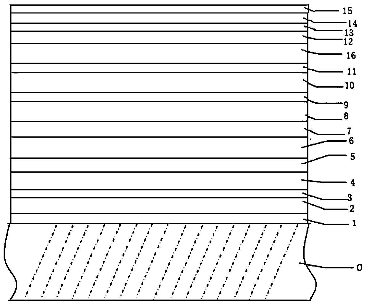
[0030] A stealth energy-saving film of the present invention is characterized in that: the stealth energy-saving film comprises a glass substrate 0, and the glass substrate 0 is sequentially composed of an electric heating functional layer, a color modulation film layer, an adhesion-enhancing film layer and a stealth film layer from the inside to the outside. functional film.
[0031] The electrical heating functional layer is sequentially from the inside to the outside as a first silicon oxide layer 1, a first tin oxide layer 2, a first metal titanium layer 3 and a second tin oxide layer 4. The film of the first silicon oxide layer 1 is The thickness of the layer is 5 nm, the thickness of the film layer of the first tin oxide layer 2 is 60 nm, the thickness of the film layer of the first metal titanium layer 3 is 9 nm, and the thickness of the film layer of the second tin oxide layer 4 is 9 nm. The thickness is 80 nm.
[0032] The color modulation film layers are, from insid...
Embodiment 2
[0042] The difference between Example 2 and Example 1 is that in a stealth energy-saving film of the present invention, the thickness of the film layer of the first silicon oxide layer 1 is 12 nm, and the thickness of the film layer of the first tin oxide layer 2 is 12 nm. 30 nm, the film thickness of the first metal titanium layer 3 is 8 nm, and the film thickness of the second tin oxide layer 4 is 60 nm.
[0043] The thickness of the indium tin nitride layer 5 is 5 nm, the thickness of the polytetrafluoroethylene layer 6 is 10 nm, the thickness of the second indium oxide layer 7 is 6 nm, and the thickness of the second indium oxide layer 8 The thickness of the film layer is 3nm;
[0044] The thickness of the tin nitride layer 9 is 10 nm, the thickness of the second silicon dioxide layer 10 is 10 nm, the thickness of the first indium oxide layer 11 is 8 nm, and the thickness of the metal gold layer 16 is 10 nm. The thickness of the film layer is 10 nm.
[0045] The thicknes...
Embodiment 3
[0053] The difference between Example 3 and Example 1 is that in a stealth energy-saving film of the present invention, the thickness of the first silicon oxide layer 1 is 15 nm, and the thickness of the first tin oxide layer 2 is 15 nm. 50 nm, the thickness of the first metal titanium layer 3 is 10 nm, and the thickness of the second tin oxide layer 4 is 75 nm.
[0054] The thickness of the indium tin nitride layer 5 is 12 nm, the thickness of the polytetrafluoroethylene layer 6 is 20 nm, the thickness of the second indium oxide layer 7 is 8 nm, and the thickness of the second indium oxide layer 8 The thickness of the film layer is 5nm;
[0055] The thickness of the tin nitride layer 9 is 5 nm, the thickness of the second silicon dioxide layer 10 is 20 nm, the thickness of the first indium oxide layer 11 is 6 nm, and the thickness of the metal gold layer 16 is 6 nm. The thickness of the film layer is 12 nm.
[0056] The thickness of the titanium nitride layer 12 is 12 nm, t...
PUM
| Property | Measurement | Unit |
|---|---|---|
| thickness | aaaaa | aaaaa |
| thickness | aaaaa | aaaaa |
| thickness | aaaaa | aaaaa |
Abstract
Description
Claims
Application Information
 - R&D Engineer
- R&D Manager
- IP Professional
- Industry Leading Data Capabilities
- Powerful AI technology
- Patent DNA Extraction
Browse by: Latest US Patents, China's latest patents, Technical Efficacy Thesaurus, Application Domain, Technology Topic, Popular Technical Reports.
© 2024 PatSnap. All rights reserved.Legal|Privacy policy|Modern Slavery Act Transparency Statement|Sitemap|About US| Contact US: help@patsnap.com


