Array substrate for thin-film transistor and display device of the same

A technology of thin-film transistors and array substrates, applied in the direction of transistors, diodes, electric solid-state devices, etc., can solve problems such as expensive and low electron mobility

Active Publication Date: 2018-04-06
LG DISPLAY CO LTD
View PDF7 Cites 0 Cited by
  • Summary
  • Abstract
  • Description
  • Claims
  • Application Information

AI Technical Summary

Problems solved by technology

Although amorphous silicon is advantageous in that the film formation process is simple and the production cost is low, its electron mobility is as low as 0.5 cm 2 The aspect of / Vs is unfavorable
Oxide semiconductor has an on / off ratio of about 108 and low leakage current, but at 10cm lower than polysilicon 2 / Vs is unfavorable in terms of electron mobility
Polysilicon has approximately 100cm 2 High electron mobility in / Vs, but disadvantageous in having a low on / off ratio compared to oxide semiconductors and applying it to a large area will be expensive

Method used


Image

  • Array substrate for thin-film transistor and display device of the same
  • Array substrate for thin-film transistor and display device of the same
  • Array substrate for thin-film transistor and display device of the same

Examples


Embodiment approach

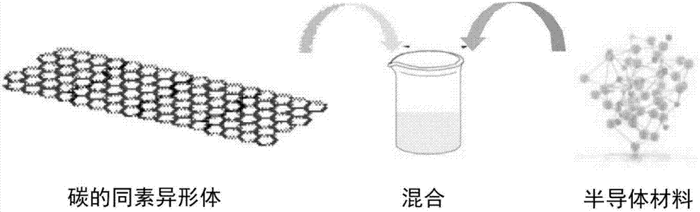
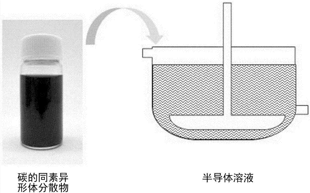
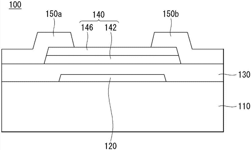
[0044] The present invention discloses a thin film transistor comprising an allotrope of carbon and a semiconductor material, and particularly discloses a thin film transistor in which an active layer comprising an allotrope of carbon and a semiconductor material is formed. Thin film transistors are used as switching elements or driving elements of display devices.

[0045]

[0046] The carbon allotropes disclosed in the present invention refer to polycyclic aromatic hydrocarbon molecules in which carbon atoms are covalently bonded to each other. The covalently bonded carbon atoms may form a 6-membered ring as a repeating unit; additionally, the covalently bonded carbon atoms may also include at least one selected from 5-membered rings and 7-membered rings. The allotrope of carbon may be a single layer, or may include multiple allotrope layers of carbon superimposed on different layers of the allotrope of carbon. Allotropes of carbon can have a one-dimensional or two-dimens...

experiment example 1

[0095] Experimental Example 1: Analysis of Active Layer Composition

[0096] The composition of the active layer consisting only of the semiconductor material, and the composition of the active layer mixed with the semiconductor material and an allotrope of carbon were subjected to Raman spectroscopic analysis. In particular, graphene is used as an allotrope of carbon, and 0.1% by weight of graphene is mixed with respect to 100% by weight of solid semiconductor material. Figure 11 A graph illustrating a Raman spectroscopic analysis result of an active layer formed of only a semiconductor material is shown, Figure 12 A graph illustrating the results of Raman spectroscopic analysis of an active layer mixed with a semiconductor material and an allotrope of carbon is shown.

[0097] refer to Figure 11 , the Raman spectroscopic analysis result of the active layer composed only of the semiconductor material showed only peaks for the substrate in which the active layer was forme...

experiment example 2

[0099] Experimental Example 2: Evaluation of Thin Film Transistors


PUM


Abstract

A thin-film transistor array substrate and a display device of the same are disclosed. The thin-film transistor array substrate, comprising a substrate, a gate electrode on the substrate, an active layer comprising a first active layer, which opposes the gate electrode and is adjacent to the gate electrode thereby comprising a semiconductor material and a plurality of carbon allotropes, and a second active layer, which is in contact with the first active layer and comprises a semiconductor material, a gate insulating film between the gate electrode and the active layer, and a source electrodeand a drain electrode respectively in contact with the active layer.

Description

technical field [0001] The invention relates to a thin film transistor array substrate and a display device comprising the thin film transistor array substrate. Background technique [0002] Recently, with the development of multimedia, the importance of flat panel display (FPD) devices is increasing. Accordingly, various displays such as Liquid Crystal Display (LCD) devices, Plasma Display Panels (PDP), Field Emission Display (FED) devices, Organic Light Emitting Display (OLED) devices are put into practical use. [0003] Methods for driving display devices include a passive matrix method and an active matrix method using thin film transistors. In the passive matrix method, anodes and cathodes are formed to be orthogonal to each other, and a row is selected for driving, while in the active matrix method, a thin film transistor is connected to each pixel electrode to perform driving according to on / off switching. [0004] Thin film transistors are very important due to the...

Claims


Application Information

Patent Timeline
Patent Type & Authority Applications(China)
IPC IPC(8): H01L27/12H01L27/32
CPCH01L27/1222H01L27/1225H10K59/1213H01L29/78669H01L29/78681H01L29/78684H01L29/7869H01L29/78696H10K10/486H01L29/78606H01L29/78618H01L29/66742H01L29/66015H10K59/50H10K59/123H10K59/124H10K19/10H10K59/125G02F1/1368H01L29/105H01L29/1054H01L29/227H01L29/24
Inventor 金昌垠白贞恩张勇均金成真
Owner LG DISPLAY CO LTD
Why Eureka
Try Eureka