Eureka AIR delivers breakthrough ideas for toughest innovation challenges, trusted by R&D personnel around the world.

A kind of oled pixel compensation circuit and its control method

A compensation circuit and pixel technology, which is applied in the field of OLED display, can solve the problems affecting the brightness of OLED pixels and the change of gate voltage of driving transistor, etc., and achieve the effect of stable brightness and stable change of gate voltage

Active Publication Date: 2019-12-03
KUNSHAN GO VISIONOX OPTO ELECTRONICS CO LTD
View PDF5 Cites 0 Cited by
  • Summary
  • Abstract
  • Description
  • Claims
  • Application Information

AI Technical Summary

Problems solved by technology

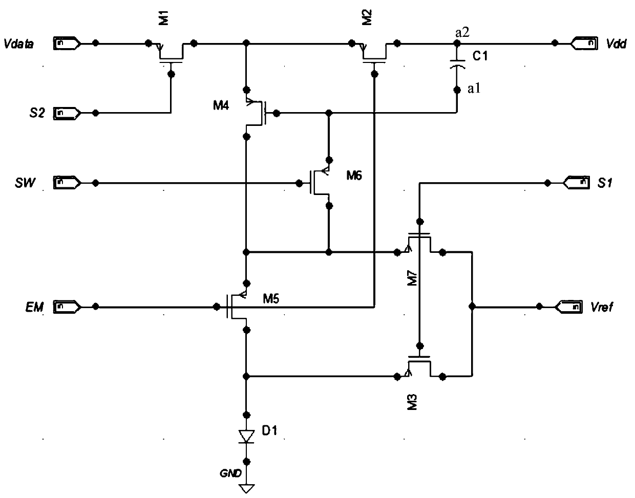
[0007] The embodiment of the present application provides an OLED pixel compensation circuit and its control method, which are used to solve the problem that the existing OLED pixel compensation circuit has a leakage path in the gate voltage of the driving transistor, which causes the gate voltage of the driving transistor to change, thereby affecting the brightness of the OLED pixel. The problem

Method used


Image

  • A kind of oled pixel compensation circuit and its control method
  • A kind of oled pixel compensation circuit and its control method
  • A kind of oled pixel compensation circuit and its control method

Examples


Embodiment Construction

[0029] In order to make the purpose, technical solution and advantages of the present application clearer, the technical solution of the present application will be clearly and completely described below in conjunction with specific embodiments of the present application and corresponding drawings. Apparently, the described embodiments are only some of the embodiments of the present application, rather than all the embodiments. Based on the embodiments in this application, all other embodiments obtained by persons of ordinary skill in the art without making creative efforts belong to the scope of protection of this application.

[0030] The specific implementation manners of the OLED pixel compensation circuit and its control method provided in the embodiments of the present application will be described in detail below with reference to the accompanying drawings.

[0031] An OLED pixel compensation circuit provided by an embodiment of the present application is as follows: ...


PUM


Abstract

The application discloses an OLED pixel compensation circuit and a control method thereof so that the grid voltage of the drive transistor changes because of a leakage path existing in the grid voltage of the drive transistor and thus the pixel brightness of the OLED is affected can be solved. The OLED pixel compensation circuit is characterized by comprising a drive transistor, a storage capacitor, a first switching transistor, a second switching transistor and a light-emitting diode. A grid electrode of the drive transistor is connected with a first terminal of the storage capacitor electrically and is connected with a source of the first switching transistor electrically; the first terminal of the storage capacitor is connected with a source of the first switching transistor electrically; a drain of the first switching transistor is connected with a source of the second switching transistor electrically; and an anode of the light-emitting diode is connected with a drain of the drivetransistor and is connected with a drain of the first switching transistor.

Description

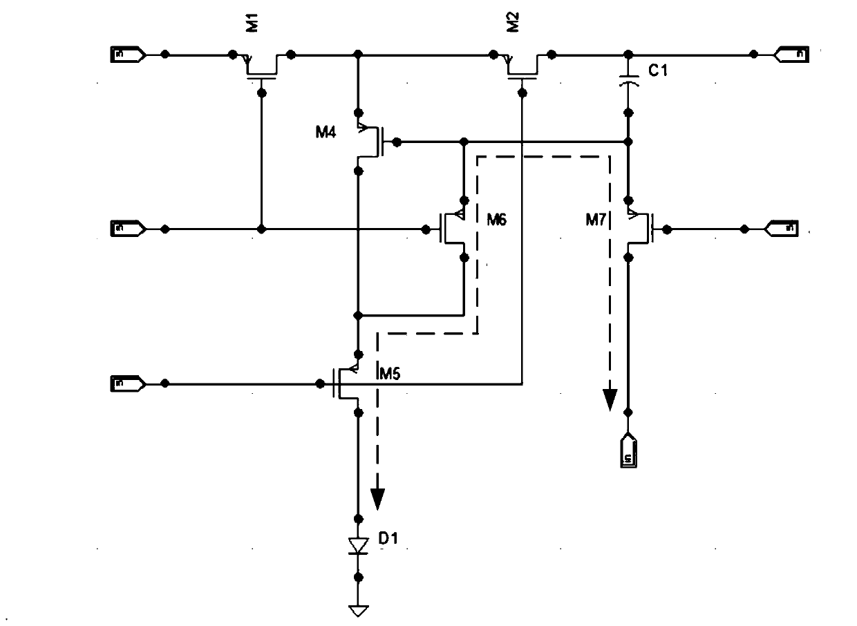
technical field [0001] The present application relates to the technical field of OLED display, in particular to an OLED pixel compensation circuit and a control method thereof. Background technique [0002] The OLED display panel prepared by using Organic Light-Emitting Display (OLED) technology has gradually become the mainstream in the field of display technology due to its advantages of small size, simple structure, high brightness, good image quality and power saving. Direction of development. [0003] However, during the use of the OLED display panel, thin film transistors (ThinFilm Transistor, TFT), which are used as switches and driving elements, may cause uneven display on the OLED display panel due to their own material characteristics. [0004] In order to solve the above problems, some manufacturers in the prior art have introduced such as figure 1 In the compensation circuit shown in the figure, C1 is a storage capacitor, M1, M2, M5, M6, and M7 are respectively...

Claims


Application Information

Patent Timeline
Patent Type & Authority Patents(China)
IPC IPC(8): G09G3/3225G09G3/3258
CPCG09G3/3225G09G3/3258G09G2320/0233
Inventor 王瑞彬
Owner KUNSHAN GO VISIONOX OPTO ELECTRONICS CO LTD
Why Eureka
Eureka Blog
Learn More