
Chip sputtering jig and sputtering method

A sputtering and jig technology, applied in the field of chip sputtering jig, can solve the problems of affecting the service life of the chip, the complex sputtering process, affecting the function of the chip, etc., to ensure the service life, save the time of sputtering, and improve the efficiency. Effect

Inactive Publication Date: 2018-03-09
丰盛印刷(苏州)有限公司
View PDF6 Cites 7 Cited by
  • Summary
  • Abstract
  • Description
  • Claims
  • Application Information

AI Technical Summary

Problems solved by technology

[0003] With the improvement of people's awareness of environmental protection, the method of using glue to smear the bottom surface of the chip and then sputtering it is gradually abandoned. Our company proposes a sputtering fixture, which is made of viscous substrates such as silica gel. , and set a through hole on the sputtering fixture, paste the chip on the sputtering fixture, after the sputtering is completed, the chip is separated from the sputtering fixture through a device such as a thimble, but there are still certain problems in this technology: first , the chip needs to be attached to the through hole, so it needs to be positioned before bonding, and the positioning accuracy needs to be ensured, which makes the sputtering process complicated and affects the sputtering efficiency; secondly, when the chip is separated from the sputtering fixture During ejection, substrates such as silica gel may remain on the bottom of the chip. In order to ensure the cleanliness of the chip, a certain amount of cleaning work is still required in the follow-up; thirdly, when ejecting, the ejector pin exerts a force on the chip, which may cause damage to the chip during subsequent use. It will affect the function of the chip, that is, a potential hidden danger, which will affect the service life of the chip

Method used


Image

  • Chip sputtering jig and sputtering method
  • Chip sputtering jig and sputtering method
  • Chip sputtering jig and sputtering method

Examples


Embodiment 1

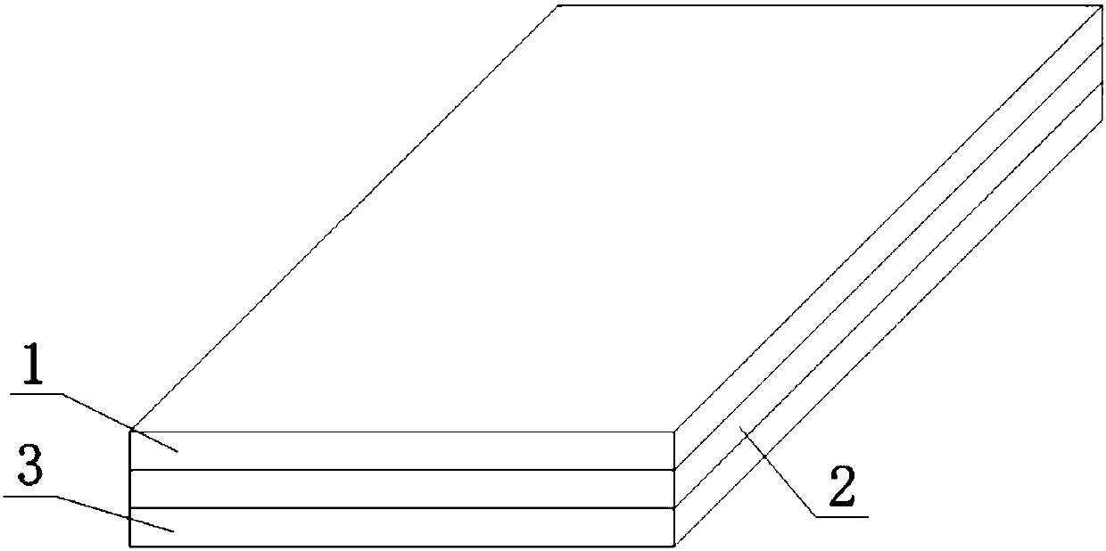
[0034] see figure 1 . The chip sputtering fixture includes an upper backing paper 1, a pyrolytic glue layer 2 and a lower backing paper 3, the pyrolytic glue layer 2 includes an upper surface and a lower surface, and the upper backing paper 1 is arranged on the pyrolytic glue The upper surface of the layer 2, the lower bottom paper 3 is arranged on the lower surface of the pyrolysis adhesive layer 2, and the upper bottom paper 1 and the lower bottom paper 3 are used to protect the pyrolysis adhesive layer 2; Layer 2 is a high-low temperature pyrolytic glue that loses its viscosity at a preset temperature, and the preset temperature of the pyrolytic glue layer 2 is higher than the sputtering temperature, so as to ensure that the pyrolytic glue layer 2 is still Has very good stickiness.

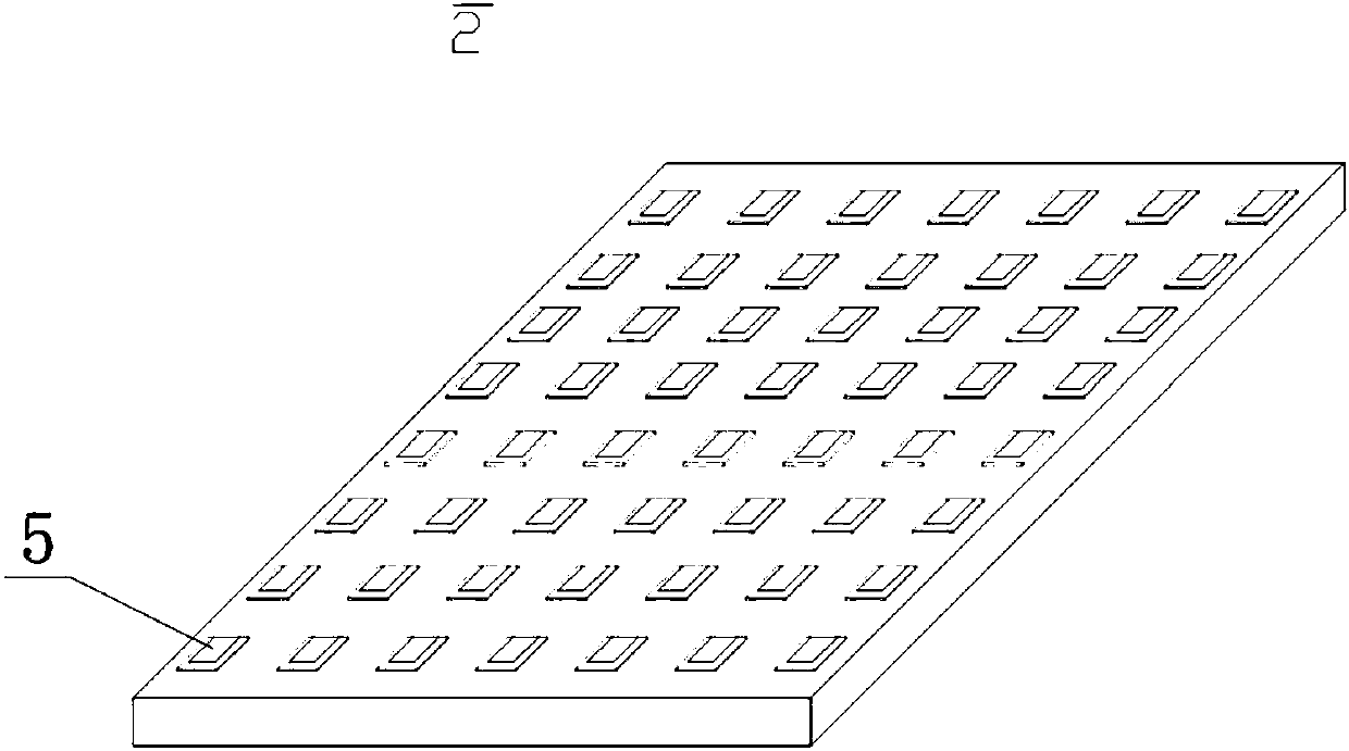
[0035] see figure 2 . The upper surface of the pyrolytic adhesive layer 2 is used to set the chip 5. Since the pyrolytic adhesive layer 2 has good viscosity at normal temperature, the chip...

Embodiment 2

[0042] see Figure 4 . The difference between this embodiment and Embodiment 1 is that the chip sputtering fixture also includes a support layer 4, and the support 4 is arranged between the pyrolytic adhesive layer 2 and the bottom paper 3, that is, the The supporting layer 4 is arranged on the lower surface of the pyrolytic adhesive layer 2 , and the bottom paper 3 is arranged on the side of the supporting layer 4 away from the pyrolytic adhesive layer 2 .

[0043] The support layer 4 includes a high-temperature-resistant Mylar sheet 40 and an adhesive layer 41, wherein the high-temperature-resistant Mylar sheet 40 is arranged on the lower surface of the pyrolytic adhesive layer 2, which has good heat resistance and is used for Supporting and protecting the pyrolytic adhesive layer 2 and the chip 5, the adhesive layer 41 is arranged between the high temperature-resistant Mylar sheet 40 and the lower backing paper 3, and is used to paste the sputtering fixture and the furnace...


PUM


Abstract

The sputtering fixture proposed by the present invention includes a pyrolytic adhesive layer, an upper backing paper, and a lower backing paper. When the sputtering fixture is used for sputtering, the upper backing paper is torn off, and the bottom surface of the chip that does not need to be sputtered is pasted on the bottom surface of the sputtering fixture. On the pyrolytic glue layer, the pyrolytic glue layer can firmly fix the chip at room temperature and during sputtering. After the sputtering is completed, the sputtering fixture is heated to a preset temperature, so that the pyrolytic glue The layer loses its stickiness, making it easy to separate the chip from the sputtering fixture. The invention can realize sputtering on five sides of the chip, and does not need positioning when pasting the chip, which simplifies the process of positioning the chip; at the same time, the chip can be easily peeled off without additional stripping process after sputtering, avoiding possible damage to the chip, The service life of the chip is guaranteed, the production cost is greatly reduced, and the sputtering efficiency is improved.

Description

technical field [0001] The invention relates to a chip sputtering fixture and a sputtering method using the sputtering fixture. Background technique [0002] A chip, as an important component of electronic equipment such as computers and mobile phones, is a small silicon chip structure that contains integrated circuits inside. Most of the chips have a cubic structure. During the manufacturing process, metal thin films need to be sputtered on the other five surfaces of the chips except the bottom to protect the chips. [0003] With the improvement of people's awareness of environmental protection, the method of using glue to smear the bottom surface of the chip and then sputtering it is gradually abandoned. Our company proposes a sputtering fixture, which is made of viscous substrates such as silica gel. , and set a through hole on the sputtering fixture, paste the chip on the sputtering fixture, after the sputtering is completed, the chip is separated from the sputtering fi...

Claims


Application Information

Patent Timeline
Patent Type & Authority Applications(China)
IPC IPC(8): C23C14/04C23C14/34H01L21/67
CPCC23C14/04C23C14/34H01L21/67011
Inventor 姜志良
Owner 丰盛印刷(苏州)有限公司
Learn More