


Quick Research
Generate reliable direction feasibility study reports for your R&D in just a few steps.

Technical Q&A
Discover and master advanced knowledge NOW. Basics, ideas, possibilities, all at once.

Find Solutions
As an expert in R&D theories, this can generate solutions to your technical problems instantly.

Evaluate Feasibility
Analyze your overall solution with one click, know your potential R&D risks in advance.

Monitor Landscape
Get weekly tech updates, stay abreast of the latest tech innovations and key insights.
Displaying device and displaying substrate
A technology for display substrates and display devices, applied in identification devices, instruments, etc., can solve the problems of reducing crack prevention, low product yield, and unclean etching of inorganic substances, so as to improve product yield and prevent the extension of cracks Effect
- Summary
- Abstract
- Description
- Claims
- Application Information
AI Technical Summary
Problems solved by technology
Method used
Image

Examples
Embodiment Construction
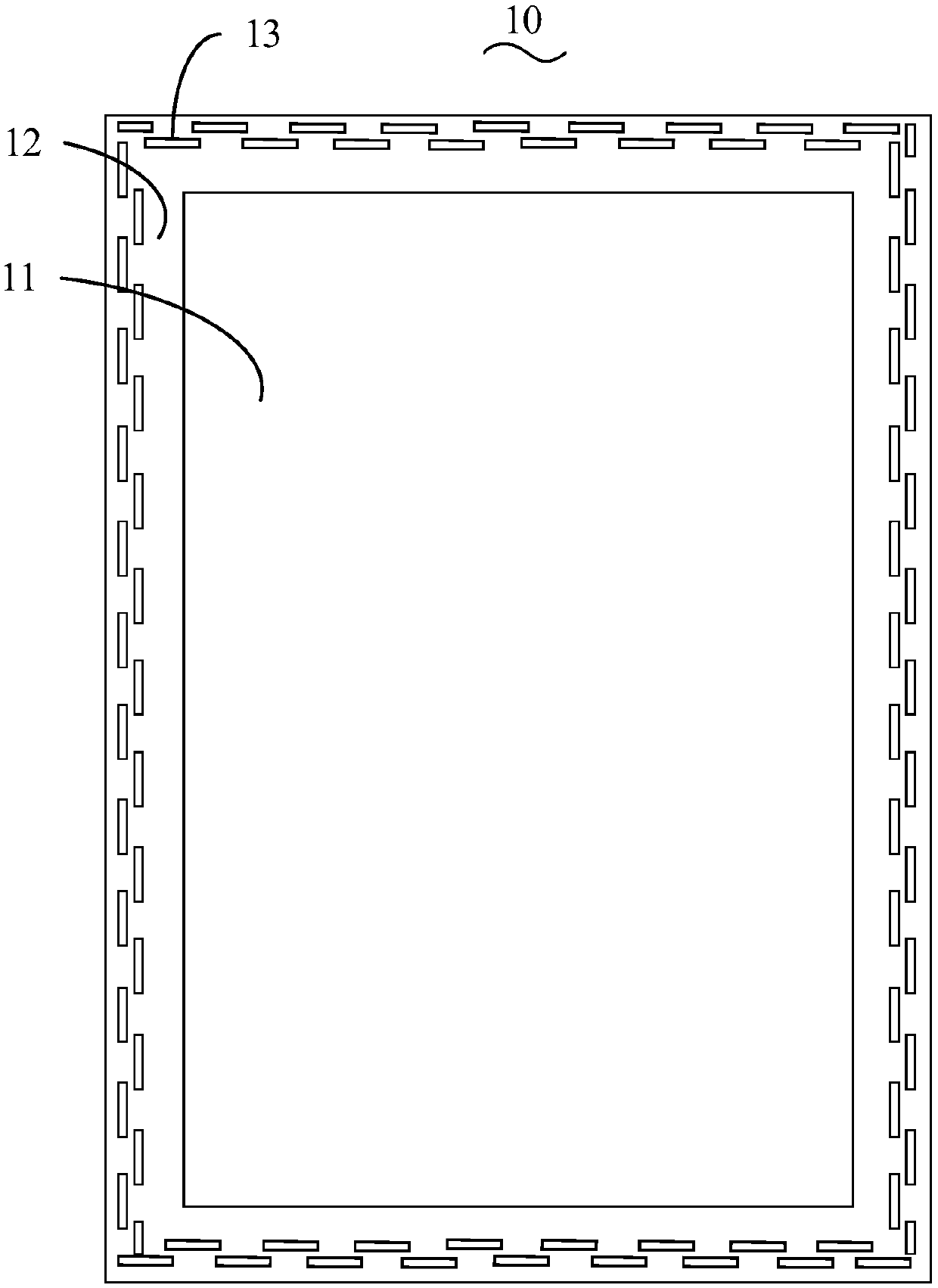
[0015] Such as figure 1 as shown, figure 1 is a schematic structural view of the display substrate according to the first embodiment of the present invention. In this embodiment, the display substrate 10 includes a display region 11 and a barrier layer 12 .
[0016] The display area 11 is located inside the display substrate 10 , and the barrier layer 12 is located between the display area 11 and the substrate edge of the display substrate 10 . Wherein, the barrier layer 12 is provided with two rows of first hole segments 13 at intervals in the direction from the display area 11 to the edge of the substrate. Each row of first hole segments 13 includes at least two first hole segments 13 arranged at intervals along the extending direction of the edge of the substrate. Moreover, projections of adjacent rows of first hole segments 13 in the extending direction of the substrate edge overlap with each other.
[0017] In this embodiment, the first hole segment 13 is arranged in ...
PUM
 Abstract
Description
Claims
Application Information
 - R&D Engineer
- R&D Manager
- IP Professional
- Industry Leading Data Capabilities
- Powerful AI technology
- Patent DNA Extraction
Browse by: Latest US Patents, China's latest patents, Technical Efficacy Thesaurus, Application Domain, Technology Topic, Popular Technical Reports.
© 2024 PatSnap. All rights reserved.Legal|Privacy policy|Modern Slavery Act Transparency Statement|Sitemap|About US| Contact US: help@patsnap.com