
Pixel defining layer and its preparation method and application

A pixel definition layer and pixel electrode technology, which is applied in semiconductor/solid-state device manufacturing, semiconductor devices, electrical components, etc., can solve problems such as lowering product yield, forming defects, and film breakage

Active Publication Date: 2020-01-24
GUANGDONG JUHUA PRINTING DISPLAY TECH CO LTD
View PDF9 Cites 1 Cited by
  • Summary
  • Abstract
  • Description
  • Claims
  • Application Information

AI Technical Summary

Problems solved by technology

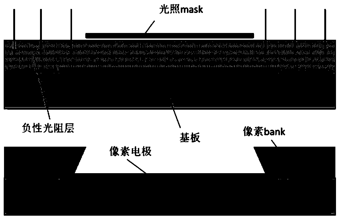
Pixel banks are generally made of photoresist materials. Negative photoresist materials are cheaper than positive photoresist materials. From the perspective of cost reduction, negative photoresists are generally used to make pixel banks. However, negative photoresist materials are used to make pixel banks. When photoresist is used to make pixel banks, it is easy to form chamfers, such as figure 1 As shown, because when the negative photoresist is exposed, the exposure dose received by the upper film is relatively larger than that of the lower film, so it is easy to form chamfers after exposure and development.
The existence of chamfering, in the later film deposition process, especially when evaporating the top electrode, is likely to cause film breakage, form defects, and reduce product yield

Method used


Image

  • Pixel defining layer and its preparation method and application
  • Pixel defining layer and its preparation method and application
  • Pixel defining layer and its preparation method and application

Examples


Embodiment Construction

[0032] In order to facilitate the understanding of the present invention, the following will describe the present invention more fully. However, the present invention can be embodied in many different forms and is not limited to the embodiments described herein. On the contrary, these embodiments are provided to make the understanding of the disclosure of the present invention more thorough and comprehensive.

[0033] Unless otherwise defined, all technical and scientific terms used herein have the same meaning as commonly understood by one of ordinary skill in the technical field of the invention. The terms used herein in the description of the present invention are for the purpose of describing specific embodiments only, and are not intended to limit the present invention. As used herein, the term "and / or" includes any and all combinations of one or more of the associated listed items.

[0034] A method for producing a pixel defining layer, the production process is as fol...


PUM


Abstract

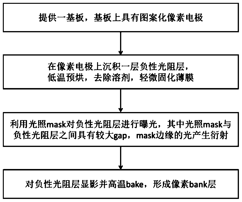
A pixel defining layer and its preparation method and application in the present invention, comprising the following steps: S1, obtaining a substrate having a patterned pixel electrode; S2, depositing a layer of negative photoresist film on the substrate; S3, Obtain a photomask, and a space is provided between the photomask and the negative photoresist film, and the space is 50-200 μm; S4, using the photomask to expose the negative photoresist film , the exposure dose is 100‑300mj / cm 2 ; S5, developing the exposed negative photoresist film to remove the unexposed negative photoresist film to form the pixel defining layer. The manufacturing method of the above-mentioned pixel defining layer can form a small tape angle by increasing the exposure distance between the photomask and the negative photoresist film during exposure. The method is simple, easy to operate and low in cost, does not cause film breakage when evaporating the top electrode, and improves product yield.

Description

technical field [0001] The invention relates to the technical field of light-emitting devices, in particular to a pixel defining layer and its preparation method and application. Background technique [0002] In the contemporary information society, the importance of the display as a visual information transmission medium is further strengthened. In order to occupy a dominant position in the future, the display is moving towards lighter, thinner, lower power consumption, lower cost and better image quality. trend development. [0003] Organic light-emitting diodes (OLEDs) have the advantages of self-luminescence, fast response, wide viewing angle, high brightness, and thinness; These advantages have become the two main directions for the development of the display field at present. [0004] At present, whether OLED or QLED is used as a light-emitting pixel unit of a display panel, it is necessary to make a pixel-defining layer (bank) in the pixel unit to define the light-e...

Claims


Application Information

Patent Timeline
Patent Type & Authority Patents(China)
IPC IPC(8): H01L51/50H01L51/52H01L51/56H01L27/32
CPCH10K59/122H10K50/115H10K50/80H10K71/00
Inventor 陈亚文
Owner GUANGDONG JUHUA PRINTING DISPLAY TECH CO LTD
Learn More