Pixel defining layer and manufacturing method thereof, display substrate, display panel

A technology of pixel definition layer and display substrate, which is applied in semiconductor/solid-state device manufacturing, semiconductor devices, electrical components, etc., can solve problems such as affecting the uniformity of solution film formation, and achieves suppression of climbing, improvement of film formation uniformity, and guarantee of The effect of stability

Active Publication Date: 2020-05-12
BOE TECH GRP CO LTD
View PDF3 Cites 0 Cited by
  • Summary
  • Abstract
  • Description
  • Claims
  • Application Information

AI Technical Summary

Problems solved by technology

[0005] Embodiments of the present invention provide a pixel defining layer and its manufacturing method, a display substrate, and a display panel, which can solve the problem of the climbing of the organic light-emitting material solution on the slope of the pixel defining layer in the related art, which affects the film formation of the solution in the pixel area. uniformity problem

Method used


Image

  • Pixel defining layer and manufacturing method thereof, display substrate, display panel
  • Pixel defining layer and manufacturing method thereof, display substrate, display panel
  • Pixel defining layer and manufacturing method thereof, display substrate, display panel

Examples


Embodiment Construction

[0057] In order to make the object, technical solution and advantages of the present invention clearer, the implementation manner of the present invention will be further described in detail below in conjunction with the accompanying drawings.

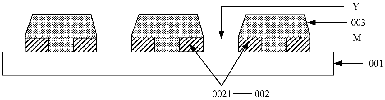
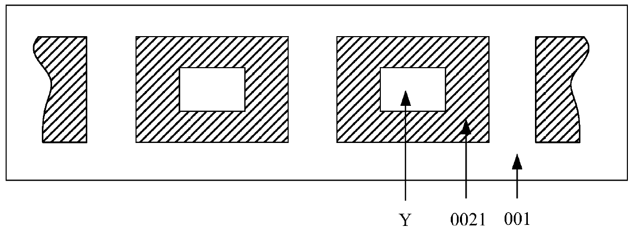
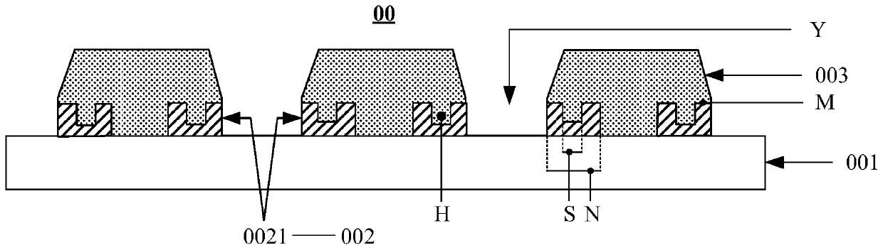
[0058] The film-forming methods of the organic light-emitting layer of the OLED display panel mainly include evaporation process and solution process. The evaporation process is relatively mature in small-scale applications, and this technology has been applied in mass production. The solution process mainly includes inkjet printing, coating, spin coating and screen printing. Among them, inkjet printing technology is considered to be an important way to achieve mass production of large-size OLEDs due to its high material utilization rate and the ability to achieve large-scale. Inkjet printing technology needs to make a pixel defining layer on the substrate with anode formed in advance, so as to limit the solution of dissolving the org...


PUM

PropertyMeasurementUnit
thicknessaaaaaaaaaa
thicknessaaaaaaaaaa
thicknessaaaaaaaaaa

Abstract

The invention discloses a pixel defining layer and a manufacturing method thereof, a display substrate and a display panel, belonging to the field of display. It includes: a lyophilic material layer arranged on the base substrate, the lyophilic material layer includes a plurality of lyophilic parts, the plurality of lyophilic parts are arranged at intervals, each of the lyophilic parts is a ring structure, And each of the lyophilic parts is used to define a pixel area; the lyophobic material layer is arranged on the side of the lyophilic material layer away from the base substrate, and the lyophobic material layer is filled in the plurality of lyophilic material layers. Between every two adjacent lyophilic parts of the liquid part, the distance from the surface of the lyophobic material layer away from the base substrate to the base substrate is greater than the distance from the surface of the lyophilic material layer away from the base substrate The distance from the surface to the substrate substrate; wherein, the lyophilic material layer is made of a lyophilic material, and the lyophobic material layer is made of a lyophobic material. The invention improves the film-forming uniformity of the solution in the pixel area. The invention is used for manufacturing display substrates of organic light emitting diodes.

Description

technical field [0001] The invention relates to the display field, in particular to a pixel defining layer and a manufacturing method thereof, a display substrate, and a display panel. Background technique [0002] An organic light-emitting diode (English: Organic Light-Emitting Diode; abbreviation: OLED) display panel includes an anode, a hole injection layer, a hole transport layer, an organic material film layer, an electron transport layer, an electron injection layer, and a cathode. Wherein, the organic material film layer can be manufactured by inkjet printing technology. When using inkjet printing technology to manufacture an organic material film layer, it is necessary to form a pixel defining layer on a glass substrate first, and then spray a solution of dissolving organic light-emitting materials onto the glass substrate on which the pixel defining layer is formed to form an organic material film layer . [0003] The pixel defining layer in the related art is mad...

Claims


Application Information

Patent Timeline
Patent Type & Authority Patents(China)
IPC IPC(8): H01L27/32H01L51/56
CPCH10K59/122H10K71/135H10K71/40H10K71/191H10K71/00
Inventor 王琳琳罗程远
Owner BOE TECH GRP CO LTD
Why Eureka
Try Eureka