Pre-solder process for printing on wafer

A wafer and pre-soldering technology, applied in the direction of electrical components, semiconductor/solid-state device manufacturing, circuits, etc., can solve problems such as welding offset, fast glue dispensing, product short circuit, etc., to prevent tin offset, The effect of reducing scrap rate and improving quality

Inactive Publication Date: 2018-01-19
东莞市佳骏电子科技有限公司
View PDF4 Cites 3 Cited by
  • Summary
  • Abstract
  • Description
  • Claims
  • Application Information

AI Technical Summary

Problems solved by technology

The defects of the existing processing method are: because the weldable area on the wafer is very small, and the speed of dispensing glue is very fast, the problem of welding offset often occurs, which leads to short circuit of the product and directly scraps the product, which greatly affects the product. the quality of

Method used


Image

  • Pre-solder process for printing on wafer
  • Pre-solder process for printing on wafer
  • Pre-solder process for printing on wafer

Examples


Embodiment Construction

[0021] In order to further understand the features, technical means, and specific objectives and functions achieved by the present invention, the present invention will be further described in detail below in conjunction with the accompanying drawings and specific embodiments.

[0022] refer to Figure 1-5 shown.

[0023] A process for printing pre-solder on a wafer, comprising the following process steps:

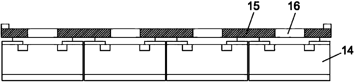
[0024] (1). Provide a full-page wafer, and place the full-page wafer 14 on the processing platform;

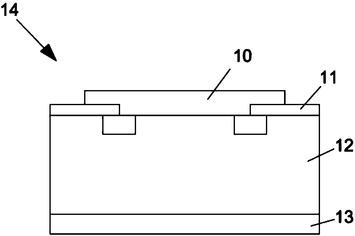
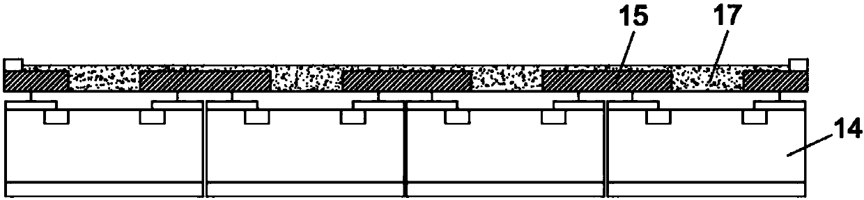
[0025] (2). Cover one deck steel mesh 15 on the P front side of wafer 14, and the mesh 16 on the steel mesh 15 corresponds to the TiNiAg layer 10 on the front side of each wafer 14P; Wherein, the steel The mesh 15 area of ​​the mesh 15 is smaller than the area of ​​the TiNiAg layer 10, and the depth of the mesh 16 is smaller than the thickness of the TiNiAg layer 10;

[0026] (3). Brush a layer of solder paste 17 on the stencil until the solder paste 17 covers the TiNiA...


PUM


Abstract

The invention provides a pre-solder process for printing on a wafer. A layer of solder paste is printed on a TiNiAg layer of the wafer by adopting a steel mesh, and then the solder paste is subjectedto reflow soldering to form solder balls. The assembly of a diode support in the later stage is facilitated. The operation is simple and convenient. The tin deflection problem of the wafer and the diode support during the welding process is avoided. Therefore, the quality of products is improved, and the rejection rate of products is reduced.

Description

technical field [0001] The invention relates to the technical field of diode processing equipment, in particular to a process for printing pre-solder on a wafer. Background technique [0002] Wafer structure reference figure 1 As shown, it includes: Ag layer 13 , Si layer 12 , SiO2 layer 11 , and TiNiAg layer 10 from bottom to top. In the prior art, ultrasonic welding and solder paste welding are generally used to integrate the chip and the diode bracket. For a wafer with a length and a width of 0.4mm, the area that can be welded is only within the range of both the length and width of 0.3mm. The existing processing method is: dot tin on the welding surface of the diode support, and then combine the wafer and the diode support into one body through reflow soldering. The defects of the existing processing method are: because the weldable area on the wafer is very small, and the speed of dispensing glue is very fast, the problem of welding offset often occurs, which leads to...

Claims


Application Information

Patent Timeline
Patent Type & Authority Applications(China)
IPC IPC(8): H01L21/48H01L21/329
Inventor 骆宗友刘忠玉
Owner 东莞市佳骏电子科技有限公司
Why Eureka
Try Eureka