Chip debugging method, device, storage medium and processor
A debugging method and a technology for configuring registers, which are applied in the field of integrated circuits, can solve problems such as low chip efficiency, and achieve the effects of solving low efficiency, alleviating the impact on area, and avoiding operation
- Summary
- Abstract
- Description
- Claims
- Application Information
AI Technical Summary
Problems solved by technology
Method used
Image

Examples
Embodiment 1
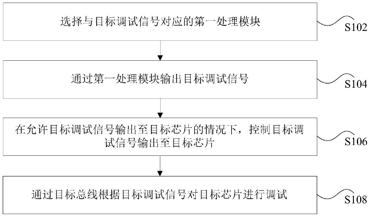
[0028] The embodiment of the present invention provides a chip debugging method.
[0029] figure 1 It is a flowchart of a chip debugging method according to an embodiment of the present invention. Such as figure 1 As shown, the method includes the following steps:
[0030] Step S102: Select the first processing module corresponding to the target debugging signal.
[0031] In the technical solution provided in step S102 of the present application, the first processing module corresponding to the target debug signal is selected, wherein the target debug signal is used to debug the target chip.
[0032] This embodiment can be used in the development of integrated circuits, and the debugging method of this embodiment can be used in the early stage of circuit design. In the debug mode (DEBUG), select the first processing module corresponding to the target debug signal. The target debugging signal is a signal required for debugging the target chip, and may be provided by a corresponding f...
Embodiment 2
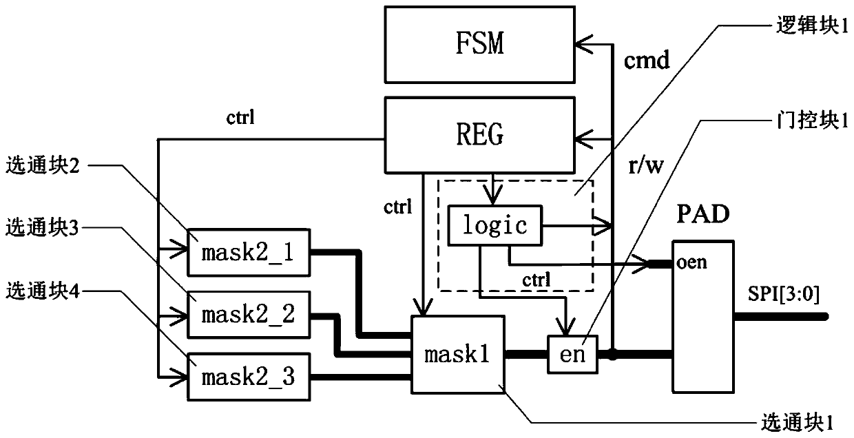
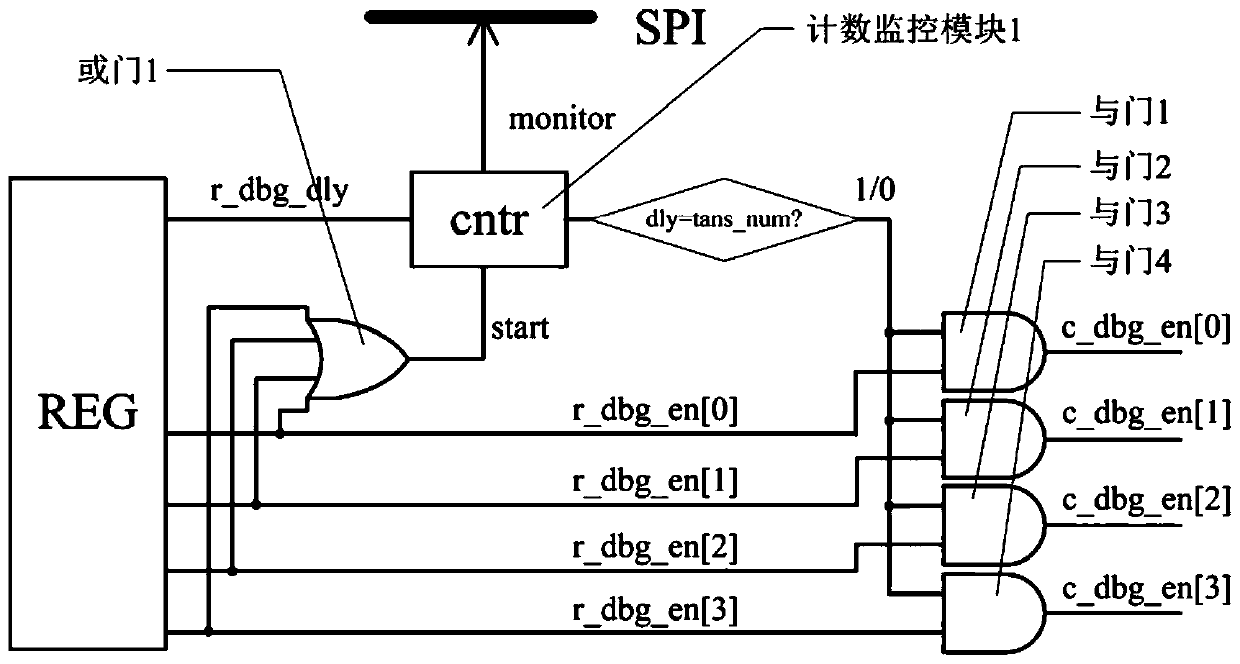
[0067] The technical solutions of the present invention will be described below in conjunction with preferred embodiments. Specifically, the target bus is an SPI bus for illustration.
[0068] figure 2 It is a schematic diagram of a chip debugging structure according to an embodiment of the present invention. Such as figure 2 As shown, in the normal working state, the external SPI[3:0] bus can read and write (r / w) the internal registers of the chip and send commands cmd through the chip port PAD. Among them, the SPI[3:0] bus Including 0, 1, 2, and 3 four lines. In the debug mode (assuming that the chip structure is composed of two levels), the gate block 1 (mask1) is controlled under the control signal ctrl through the configuration register REG to select the processing module where the required signal is located; through the configuration register REG under the control signal ctrl Gate block 2 (mask2_1) selects the signal in the processing module for output; configures REG t...
Embodiment 3
[0072] The embodiment of the invention also provides a chip debugging device. It should be noted that the chip debugging device of this embodiment can be used to execute the chip debugging method of the embodiment of the present invention.
[0073] Figure 4 It is a schematic diagram of a chip debugging device according to an embodiment of the present invention. Such as Figure 4 As shown, the device includes: a selection unit 10, an output unit 20, a control unit 30, and a debugging unit 40.
[0074] The selection unit 10 is configured to select the first processing module corresponding to the target debug signal, where the target debug signal is used to debug the target chip.
[0075] The output unit 20 is configured to output the target debugging signal through the first processing module.
[0076] The control unit 30 is configured to control the target debugging signal to be output to the target chip when the target debugging signal is allowed to be output to the target chip, w...
PUM
 Abstract
Description
Claims
Application Information
 - R&D
- Intellectual Property
- Life Sciences
- Materials
- Tech Scout
- Unparalleled Data Quality
- Higher Quality Content
- 60% Fewer Hallucinations
Browse by: Latest US Patents, China's latest patents, Technical Efficacy Thesaurus, Application Domain, Technology Topic, Popular Technical Reports.
© 2025 PatSnap. All rights reserved.Legal|Privacy policy|Modern Slavery Act Transparency Statement|Sitemap|About US| Contact US: help@patsnap.com