Simple screen plate manufacturing method suitable for pasting chip

A production method and screen technology, which is applied in the direction of assembling printed circuits with electrical components, can solve problems such as difficult to guarantee welding quality, waste of funds and resources, and low production efficiency, and achieve reduced steel mesh scrapping, high production efficiency, and high processing efficiency. convenient effect

Inactive Publication Date: 2018-01-16
JIANGXI KAIQIANG IND CO LTD
View PDF4 Cites 2 Cited by
  • Summary
  • Abstract
  • Description
  • Claims
  • Application Information

AI Technical Summary

Problems solved by technology

[0002] For flexible circuit board samples that require soldering of components, since the number of components to be soldered for each piece of product is increasing, and the size of components is getting smaller and smaller, manual soldering is not only extremely low in production efficiency At the same time, the welding quality is becoming more and more difficult to guarantee, so the manual welding method is rarely used for the welding of the components of the flexible circuit board sample, and the way of using SMT patch is the best way to ensure the welding quality of the components
However, due to the small quantity of each sample and the large number of models, SMT patches need to make stencils for solder paste printing, and the overall cost will be quite high. In the market, the average price of stencils for each sample is 250 Yuan calculation (the price of a simple steel mesh is generally around 200 yuan, while the price of a complex steel mesh will reach 300-500 yuan a piece)
In daily use, samples are uncertain (that is, there may be subsequent optimization and changes), and the proportion of samples that can be converted into batches is generally only about 30%. Once samples are changed, optimized, or samples cannot be converted into batches, All the stencils opened will be completely waste products, which will cause waste of stencils, resulting in a great waste of funds and resources

Method used


Image

  • Simple screen plate manufacturing method suitable for pasting chip

Examples


Embodiment 1

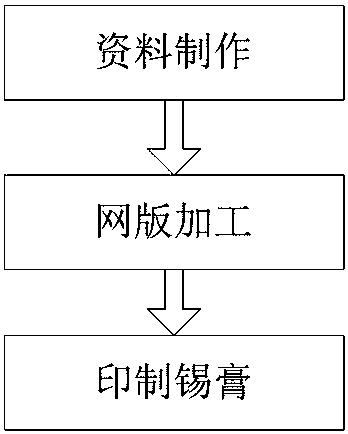
[0024] Such as figure 1 As shown, the invention discloses a method for making a simple screen suitable for patching, comprising the following steps:

[0025] A. Data production, including laser cutting quality production and FR4 board drilling quality production:

[0026] Production of laser cutting data: first copy the steel mesh laser cutting data to the simple screen laser cutting data, and then design a simple screen positioning hole according to the position of the positioning holes around the product, the aperture is ¢1.98mm;

[0027] Production of FR4 board drilling data: design FR4 positioning holes according to the positioning holes around the product, with a diameter of ¢1.98mm;

[0028] B. Processing the screen, cutting two double-sided substrates and FR4 boards of the same size;

[0029] The width of the double-sided substrate is 250mm, the length is 10mm larger than the length of the product, and the thickness is controlled at 50um. The graphic window and positi...

Embodiment 2

[0033] Such as figure 1 As shown, the invention discloses a method for making a simple screen suitable for patching, comprising the following steps:

[0034] A. Data production, including laser cutting quality production and FR4 board drilling quality production:

[0035] Production of laser cutting data: first copy the steel mesh laser cutting data to the simple screen laser cutting data, and then design a simple screen positioning hole according to the position of the positioning holes around the product, the aperture is ¢1.98mm;

[0036] Production of FR4 board drilling data: design FR4 positioning holes according to the positioning holes around the product, with a diameter of ¢1.98mm;

[0037] B. Processing the screen, cutting two double-sided substrates and FR4 boards of the same size;

[0038] The width of the double-sided substrate is 250mm, the length is 10mm larger than the length of the product, and the thickness is controlled at 100u. The graphic window and positi...

Embodiment 3

[0042] Such as figure 1 As shown, the invention discloses a method for making a simple screen suitable for patching, comprising the following steps:

[0043] A. Data production, including laser cutting quality production and FR4 board drilling quality production:

[0044] Production of laser cutting data: first copy the steel mesh laser cutting data to the simple screen laser cutting data, and then design a simple screen positioning hole according to the position of the positioning holes around the product, the aperture is ¢1.98mm;

[0045] Production of FR4 board drilling data: design FR4 positioning holes according to the positioning holes around the product, with a diameter of ¢1.98mm;

[0046] B. Processing the screen, cutting two double-sided substrates and FR4 boards of the same size;

[0047] The width of the double-sided substrate is 250mm, the length is 10mm larger than the length of the product, and the thickness is controlled at 60um. The graphic window and positi...


PUM


Abstract

The invention discloses a simple screen plate manufacturing method suitable for pasting a chip, and the method comprises the following steps: A, data making: carrying out the making of laser cutting data and the making of FR4 plate drilling data, so as to design a simple screen plate positioning hole and an FR4 plate positioning hole; B, screen plate machining: carrying out the rough shape cuttingof a double-side substrate and an FR4 plate which are the same in size, machining the double-side substrate according to the laser cutting data, and machining the FR4 plate according to the FR4 platedrilling data; C, solder paste printing: taking a flexible circuit board to serve as a to-be-processed product, enabling a positioning hole of the product to be aligned with the positioning hole of the FR4 plate and to be disposed on the FR4 plate in a sleeved manner, enabling the cut double-side substrate to sleeve the product in a direction, printing solder paste on the product in a mode of manual printing, and obtaining a simple screen plate which is suitable for pasting the chip. The method is high in production efficiency, is high in adaptability, is low in cost, and is convenient to process.

Description

technical field [0001] The invention relates to the technical field of printed circuit board processing, in particular to a method for making a simple screen plate suitable for patching. Background technique [0002] For flexible circuit board samples that require soldering of components, since the number of components to be soldered for each piece of product is increasing, and the size of the components is getting smaller and smaller, the manual soldering method is not only extremely low in production efficiency , At the same time, it is becoming more and more difficult to guarantee the welding quality, so the manual welding method is rarely used for the welding of the components of the flexible circuit board sample, and the SMT chip is the best way to ensure the welding quality of the components. However, due to the small number of samples of each model and the large number of models, SMT patches need to make stencils for solder paste printing, and the overall cost will be...

Claims


Application Information

Patent Timeline
Patent Type & Authority Applications(China)
IPC IPC(8): H05K3/34
Inventor 吴斌李彬
Owner JIANGXI KAIQIANG IND CO LTD
Why Eureka
Try Eureka