Scanning drive circuit and display panel for light-emitting diode display

A scan drive circuit and scan drive technology, applied to static indicators, instruments, etc., can solve problems such as complex implementation process and drive mode, threshold voltage drift, and display brightness differences, so as to improve display effects, reduce differences, and solve problems. drift effect

Active Publication Date: 2019-08-30
SHENZHEN CHINA STAR OPTOELECTRONICS SEMICON DISPLAY TECH CO LTD
View PDF10 Cites 0 Cited by
  • Summary
  • Abstract
  • Description
  • Claims
  • Application Information

AI Technical Summary

Problems solved by technology

However, during use, due to the long-term pressure and high temperature of the thin-film transistor TFT, its threshold voltage will drift. Due to different display screens, the threshold drift of each part of the TFT panel will be different, which will cause differences in display brightness. In order to solve this One problem, on the basis of the original signal, the internal compensation signal of AMOLED is added
[0003] The inventors of the present invention have found in the course of long-term research, such as figure 1 As shown, in the prior art, it is necessary to use a sub-circuit constructed by TFT inside the pixel to solve this problem. The method of generating a compensation signal by adding an additional circuit has a relatively complicated implementation process and driving method.

Method used


Image

  • Scanning drive circuit and display panel for light-emitting diode display
  • Scanning drive circuit and display panel for light-emitting diode display
  • Scanning drive circuit and display panel for light-emitting diode display

Examples


Embodiment Construction

[0015] The present invention will be described in detail below in conjunction with the accompanying drawings and embodiments.

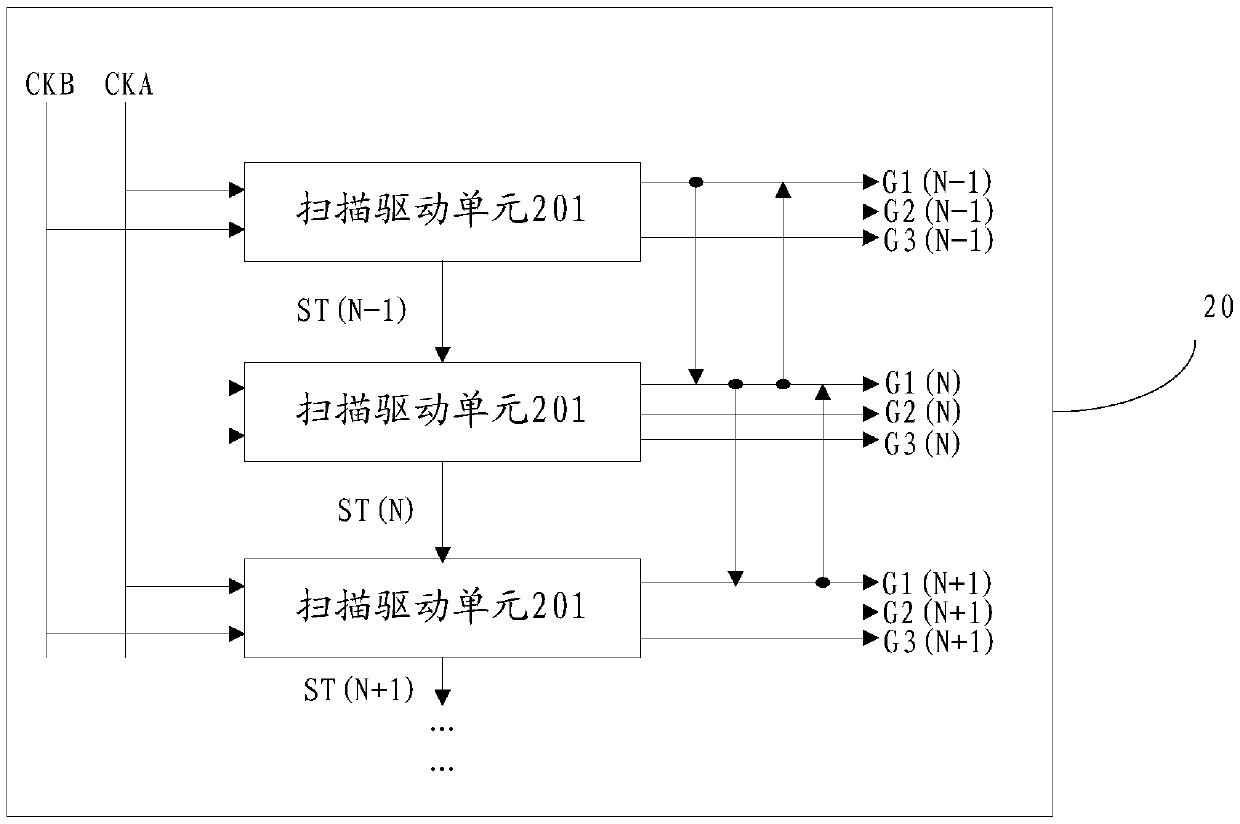
[0016] see figure 2 , figure 2 It is a structural schematic diagram of an embodiment of the scanning driving circuit of the present invention. As shown in the figure, the scanning driving circuit 20 includes a plurality of cascaded scanning driving units 201 .

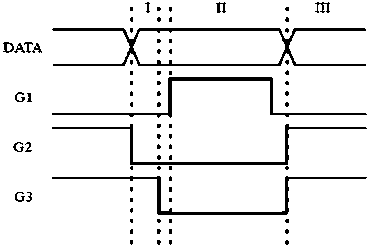
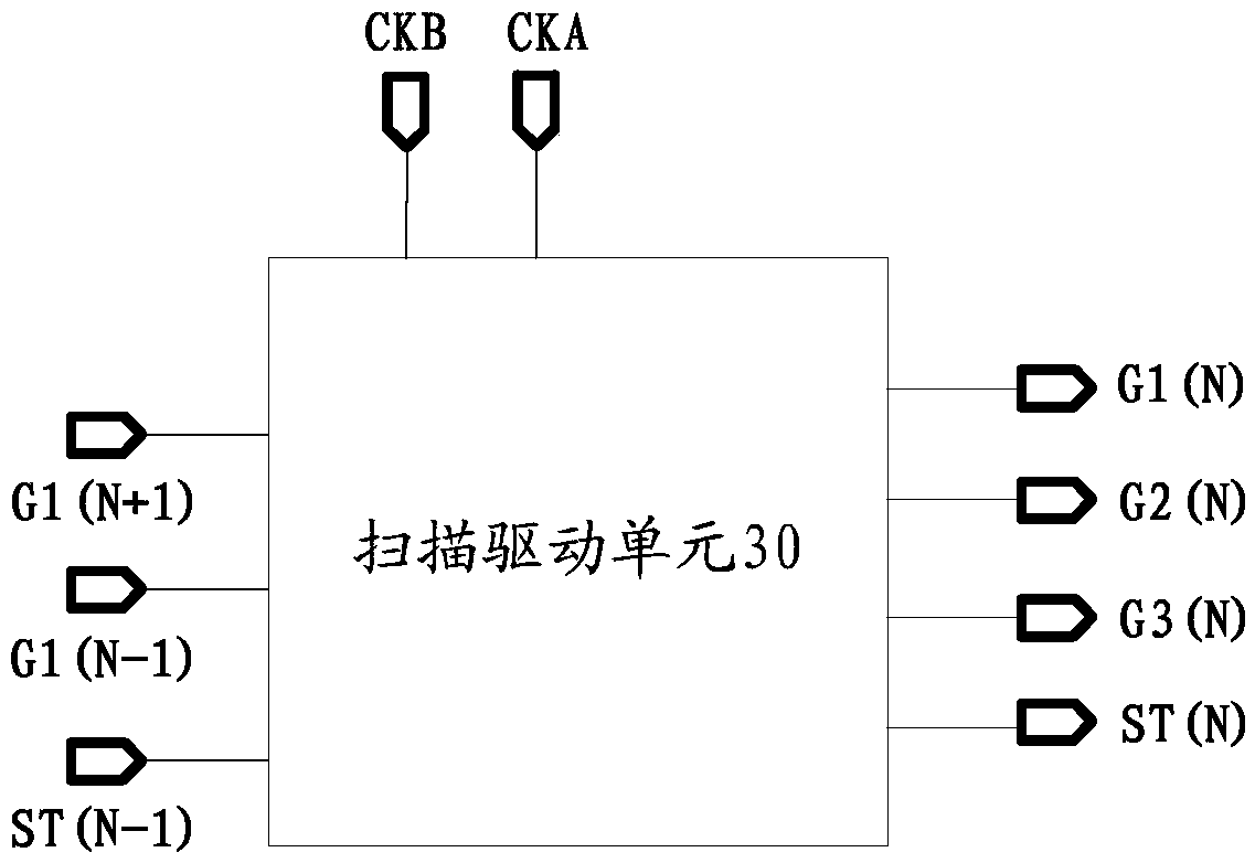
[0017] see image 3 , image 3 It is a schematic diagram of the circuit principle of an embodiment of the scanning drive unit of the present invention. like image 3 As shown, the scan driving unit 30 in this embodiment is used to receive the upper-level step-by-step signal ST(N-1), the upper-level first scan signal G1(N-1), the lower-level first scan signal G1( N+1), the first clock signal CKA and the second clock signal CKB to output the stage transmission signal ST (N), the first scanning signal G1 (N) of the stage, and the second scanning signal G2 (N) of the stage The duty cycle o...


PUM


Abstract

A scanning driving circuit (20, 701) for a light emitting diode display, and a display panel (70). The scanning driving circuit (20, 701) comprises a plurality of scanning driving units (30) in cascade connection; each stage of the scanning driving units (30) is used for receiving a stage transmission signal of the previous stage (ST(N-1)), a first scanning signal of the previous stage (G1(N-1)), a first scanning signal of the next stage (G1(N+1)), a first clock signal (CKA), and a second clock signal (CKB), and outputting a stage transmission signal of the current stage (ST(N)), a first scanning signal of the current stage (G1(N)), a second scanning signal of the current stage (G2(N)), and a third scanning signal of the current stage (G3(N)), wherein the duty ratios of the first clock signal (CKA) and the second clock signal (CKB) are different. The scanning driving circuit (20, 701) can generate three types of shift scanning signals required by a pixel compensation circuit, so that the problem of threshold-voltage drift can be resolved, thereby further reducing the difference in display brightness, and improving the display effect.

Description

technical field [0001] The invention relates to the technical field of displays, in particular to a scanning driving circuit and a display panel for light-emitting diode display. Background technique [0002] Flat-panel display devices have many advantages such as thin body, power saving, and no radiation, and have been widely used. Existing flat panel display devices mainly include liquid crystal display (Liquid Crystal Display, LCD) and organic light emitting diode display (Organic Light Emitting Display, OLED), and active matrix organic light emitting diode (Active-matrix organic light emitting diode, AMOLED) has significant advantages over LCD in terms of energy consumption, color saturation, contrast, and flexible applications, and is widely used. However, during use, due to the long-term pressure and high temperature of the thin-film transistor TFT, its threshold voltage will drift. Due to different display screens, the threshold drift of each part of the TFT panel wi...

Claims


Application Information

Patent Timeline
Patent Type & Authority Patents(China)
IPC IPC(8): G09G3/3266
Inventor 曾勉
Owner SHENZHEN CHINA STAR OPTOELECTRONICS SEMICON DISPLAY TECH CO LTD
Why Eureka
Try Eureka