
Pixel circuit control method, pixel circuit control circuit and display device

A technology of pixel circuits and control circuits, applied in static indicators, instruments, etc., can solve the problems of decreased current efficiency, drift of electrical parameters of driving transistors, and long time period of driving light-emitting elements to emit light.

Inactive Publication Date: 2018-01-16
BOE TECH GRP CO LTD
View PDF12 Cites 8 Cited by
  • Summary
  • Abstract
  • Description
  • Claims
  • Application Information

AI Technical Summary

Problems solved by technology

[0004] The inventors have found through research that the driving transistor drives the light-emitting element to emit light for a long period of time, causing the driving transistor and OLED to be in a forward-biased state for a long time, which not only causes the drift of the electrical parameters inside the driving transistor and OLED and reduces the lifetime, but also lead to a drop in current efficiency

Method used


Image

  • Pixel circuit control method, pixel circuit control circuit and display device
  • Pixel circuit control method, pixel circuit control circuit and display device
  • Pixel circuit control method, pixel circuit control circuit and display device

Examples


Embodiment 1

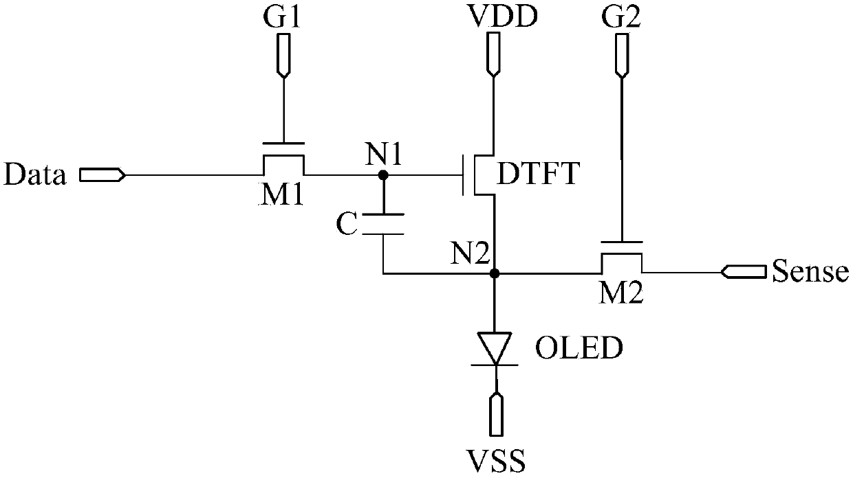
[0041] figure 1 A flow chart of a method for controlling a pixel circuit provided in an embodiment of the present invention, wherein the pixel circuit includes: a driving transistor for driving a light-emitting element, such as figure 1 As shown, the pixel circuit control method provided by the embodiment of the present invention specifically includes:

[0042]Step 100: Input a first control signal to the input terminal of the pixel circuit during the reverse bias period, so that the light emitting element and the driving transistor reverse bias the input terminal of the pixel circuit to input the first control signal.

[0043] It should be noted that the timing of the control signal includes: driving the display phase and a non-display phase, the non-display phase includes a reverse bias time period, and the reverse bias time period in the embodiment of the present invention is pre-selected in the non-display phase period.

[0044] Optionally, the light emitting element may...

Embodiment 2

[0079] Based on the inventive concepts of the above-mentioned embodiments, the embodiment of the present invention provides a control circuit for a pixel circuit, which is implemented by applying the control method for a pixel circuit provided in Embodiment 1. The pixel circuit includes a driving transistor for driving a light-emitting element to emit light, and a control signal The timing includes: driving a display phase and a non-display phase, and the non-display phase includes a reverse bias time period; the control circuit is connected to the input terminal of the pixel circuit, and is configured to input to the pixel circuit during the reverse bias time period The terminal inputs the first control signal to reverse bias the light emitting element and the driving transistor.

[0080] It should be noted that the reverse bias time period in the embodiment of the present invention is a pre-selected time period in the non-display phase.

[0081] Optionally, the light emittin...


PUM


Abstract

The embodiment of the invention provides a pixel circuit control method, a pixel circuit control circuit and a display device. The pixel circuit control method comprises the steps that a time sequenceof a control signal comprises a driving display stage and a non-display stage, wherein the non-display stage comprises a reverse bias time period; and a first control signal is inputted into an inputend of a pixel circuit in the reverse bias time period so as to enable a light emitting element and a driving transistor to be reversely biased, wherein the reverse bias period is a time period pre-selected in the non-display stage. According to the embodiment of the invention, electrons captured by the light emitting element and the driving transistor in forward bias can be partially recovered through achieving reverse bias for the light emitting element and the driving transistor in the reverse bias time period, thereby not only realizing electrical parameter drifting and current efficiencyrecovery inside the driving transistor and the OLED, but also prolonging the life of the driving transistor and the OLED.

Description

technical field [0001] Embodiments of the present invention relate to the field of display technology, and in particular to a method for controlling a pixel circuit, a control circuit thereof, and a display device. Background technique [0002] Organic Light-Emitting Diode (OLED) is one of the hot spots in the field of flat panel display research. Compared with Liquid Crystal Display (LCD), OLED display has low energy consumption, low production cost, self-luminous , wide viewing angle and fast response speed, etc. At present, OLED displays have begun to replace traditional LCD displays in the display fields of mobile phones, tablet computers, and digital cameras. [0003] Unlike LCD, which uses a stable voltage to control brightness, OLED is current-driven and requires a stable current to control the light. Generally, an OLED display outputs current to the OLED through a driving transistor in a pixel circuit in each pixel, so as to drive the OLED to emit light. [0004] T...

Claims


Application Information

Patent Timeline
IPC IPC(8): G09G3/3208
CPCG09G3/3233G09G2320/0233G09G2320/0238G09G2320/0295G09G2320/045G09G2330/021G09G2310/08
Inventor 李全虎王玲杨栋芳闫光
Owner BOE TECH GRP CO LTD
Learn More