Electromagnetic shielding package body and manufacturing method

An electromagnetic shielding and shielding body technology, which is applied in semiconductor/solid-state device manufacturing, electric solid-state devices, circuits, etc., can solve problems such as high cost, unfavorable heat dissipation of the plastic sealing layer, complexity, etc., to achieve the elimination of electromagnetic interference, simple manufacturing, good electromagnetic The effect of isolation

Active Publication Date: 2017-12-08
NAT CENT FOR ADVANCED PACKAGING
View PDF4 Cites 6 Cited by
  • Summary
  • Abstract
  • Description
  • Claims
  • Application Information

AI Technical Summary

Problems solved by technology

The disadvantage of this solution is that it is a high-cost and complicated process to equip each chip with a large-area plastic packaging layer covering the entire chip. In addition, the plastic packaging layer is not conducive to heat dissipation.

Method used


Image

  • Electromagnetic shielding package body and manufacturing method
  • Electromagnetic shielding package body and manufacturing method
  • Electromagnetic shielding package body and manufacturing method

Examples


Embodiment Construction

[0035] It should be noted that components in the various figures may be shown exaggerated for the purpose of illustration and are not necessarily true to scale. In the various figures, identical or functionally identical components are assigned the same reference symbols.

[0036] Unless otherwise specified, in this application, the quantifiers "a" and "an" do not exclude the scene of multiple elements.

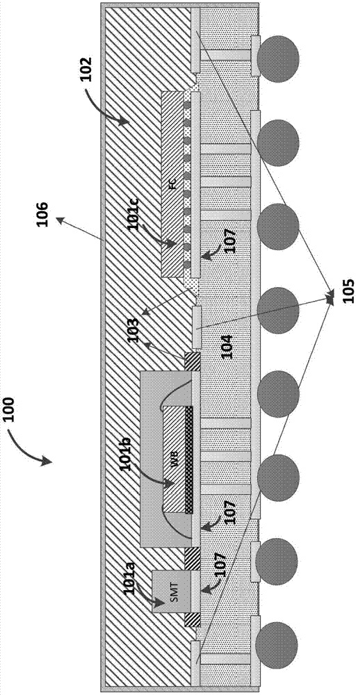
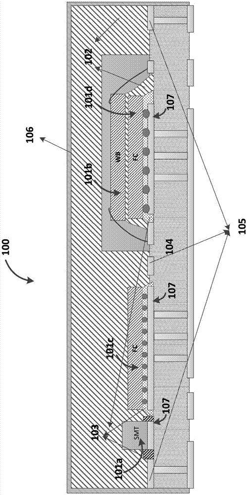
[0037] figure 1 A schematic diagram of a first embodiment of the electromagnetic shielding package 100 according to the present invention is shown.

[0038] Such as figure 1 As shown, the electromagnetic shielding package 100 includes a substrate 104 . The substrate 104 may be, for example, a common printed circuit board (PCB). The substrate 104 may include various conductive structures, such as interconnection lines 107 for connecting the chips 101a, 101b and 101c, and grounding lines 105 for grounding the shield 102, or may also include via holes (not shown). These con...


PUM


Abstract

The invention relates to an electromagnetic shielding package body which includes: a substrate; at least two chips which are disposed on the substrate; a shielding body which is made of a shielding gel and covers the chips and separate the chips from one another so as to provide electromagnetic shielding between the chips and the environment and among the chips, wherein the shielding body is grounded through a conductor; and an insulating layer which is made of an insulating gel, wherein the insulating layer is coated to a conductive structure of the chips, in supposedly electrical insulation from the shielding body, and / or is coated to a conductive structure of the substrate, in supposedly electrical insulation from the shielding body, such that the conductive structure and the shielding body are electrically insulated. The invention also relates to a method for manufacturing such electromagnetic shielding package body.

Description

technical field [0001] The present invention relates to the field of semiconductor manufacturing, in particular to an electromagnetic shielding package and a method for manufacturing such a package. Background technique [0002] As the requirements for portability, low weight, and small size of electronic products continue to increase, system-in-package (SiP) technology has been vigorously developed. An important development trend of system-in-package is to package different chips such as high-speed digital circuits, analog circuits and radio frequency circuits in one package to achieve the required integration level. However, this creates the problem of electromagnetic interference between the chips in the package and the problem of electromagnetic radiation outside the package. [0003] A solution to the electromagnetic radiation problem is to use a metal shield. Such a shielding case usually consists of a frame with isolation walls and a cover, wherein the isolation wal...

Claims


Application Information

Patent Timeline
IPC IPC(8): H01L23/31H01L23/552H01L21/50H01L21/56
CPCH01L23/552H01L21/50H01L21/56H01L23/3114H01L23/3128H01L2924/181H01L2924/19105H01L2224/16225H01L2224/32145H01L2224/48091H01L2224/73204H01L2224/73265H01L2924/00014H01L2924/00012
Inventor 李君张绪
Owner NAT CENT FOR ADVANCED PACKAGING
Why Eureka
Try Eureka