


Quick Research
Generate reliable direction feasibility study reports for your R&D in just a few steps.

Technical Q&A
Discover and master advanced knowledge NOW. Basics, ideas, possibilities, all at once.

Find Solutions
As an expert in R&D theories, this can generate solutions to your technical problems instantly.

Evaluate Feasibility
Analyze your overall solution with one click, know your potential R&D risks in advance.

Monitor Landscape
Get weekly tech updates, stay abreast of the latest tech innovations and key insights.
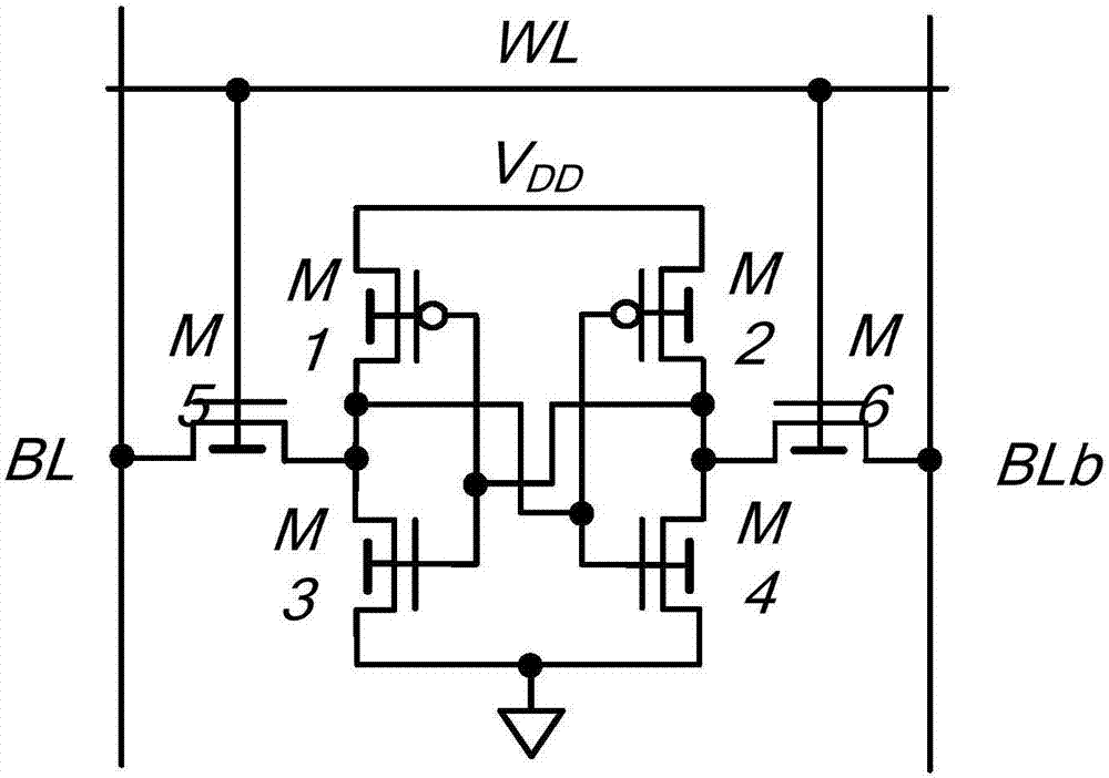
FinFET device-based full-swing single-end read storage unit
A storage unit, full swing technology, applied in information storage, static memory, digital memory information and other directions, can solve the problems of unstable circuit function, large delay, destroying the data value of the storage point, etc., to improve the sensitivity and improve the noise. The effect of tolerance
- Summary
- Abstract
- Description
- Claims
- Application Information
AI Technical Summary
Problems solved by technology
Method used
Image

Examples
Embodiment 1
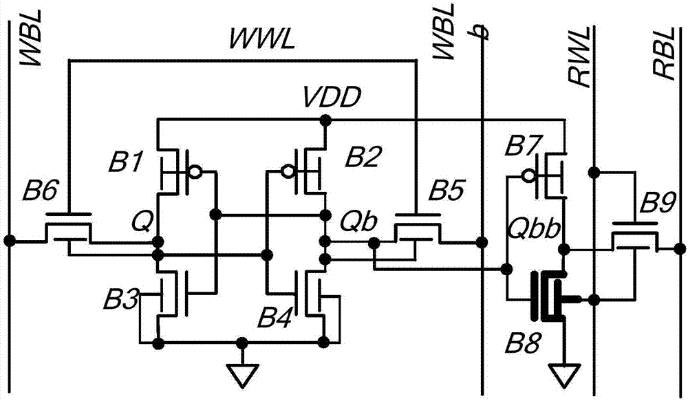
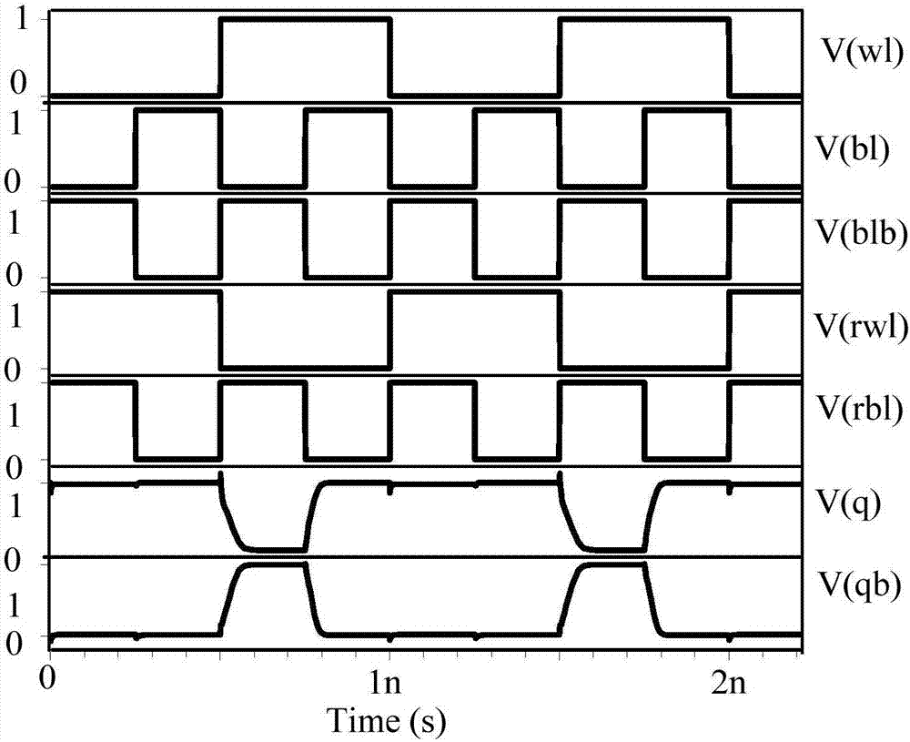
[0015] Embodiment one: if figure 2As shown, a read decoupling memory unit based on a FinFET device includes a write word line WWL, a write bit line WBL, an inverted write bit line WBLb, a read word line RWL, a read bit line RBL, a first FinFET tube B1, a second FinFET B2, third FinFET B3, fourth FinFET B4, fifth FinFET B5, sixth FinFET B6, seventh FinFET B7, eighth FinFET B8, ninth FinFET B9, first FinFET B1, the second FinFET tube B2 and the seventh FinFET tube B7 are respectively low-threshold P-type FinFET tubes, the third FinFET tube B3, the fourth FinFET tube B4, the fifth FinFET tube B5, the sixth FinFET tube B6 and the ninth FinFET tube Tube B9 is an N-type FinFET tube with a low threshold, the eighth FinFET tube B8 is an N-type FinFET tube with a high threshold, the source of the first FinFET B1, the source of the second FinFET B2, and the seventh FinFET B7 The source of the read decoupling storage unit is connected to the power supply terminal of the read decoupling...
Embodiment 2
[0016] Embodiment two: if figure 2 As shown, a read decoupling memory unit based on a FinFET device includes a write word line WWL, a write bit line WBL, an inverted write bit line WBLb, a read word line RWL, a read bit line RBL, a first FinFET tube B1, a second FinFET B2, third FinFET B3, fourth FinFET B4, fifth FinFET B5, sixth FinFET B6, seventh FinFET B7, eighth FinFET B8, ninth FinFET B9, first FinFET B1, the second FinFET tube B2 and the seventh FinFET tube B7 are respectively low-threshold P-type FinFET tubes, the third FinFET tube B3, the fourth FinFET tube B4, the fifth FinFET tube B5, the sixth FinFET tube B6 and the ninth FinFET tube Tube B9 is an N-type FinFET tube with a low threshold, the eighth FinFET tube B8 is an N-type FinFET tube with a high threshold, the source of the first FinFET B1, the source of the second FinFET B2, and the seventh FinFET B7 The source of the read decoupling storage unit is connected to the power supply terminal of the read decouplin...
Embodiment 3
[0018] Embodiment three: as figure 2 As shown, a read decoupling memory unit based on a FinFET device includes a write word line WWL, a write bit line WBL, an inverted write bit line WBLb, a read word line RWL, a read bit line RBL, a first FinFET tube B1, a second FinFET B2, third FinFET B3, fourth FinFET B4, fifth FinFET B5, sixth FinFET B6, seventh FinFET B7, eighth FinFET B8, ninth FinFET B9, first FinFET B1, the second FinFET tube B2 and the seventh FinFET tube B7 are respectively low-threshold P-type FinFET tubes, the third FinFET tube B3, the fourth FinFET tube B4, the fifth FinFET tube B5, the sixth FinFET tube B6 and the ninth FinFET tube Tube B9 is an N-type FinFET tube with a low threshold, the eighth FinFET tube B8 is an N-type FinFET tube with a high threshold, the source of the first FinFET B1, the source of the second FinFET B2, and the seventh FinFET B7 The source of the read decoupling storage unit is connected to the power supply terminal of the read decoupl...
PUM
 Abstract
Description
Claims
Application Information
 - R&D Engineer
- R&D Manager
- IP Professional
- Industry Leading Data Capabilities
- Powerful AI technology
- Patent DNA Extraction
Browse by: Latest US Patents, China's latest patents, Technical Efficacy Thesaurus, Application Domain, Technology Topic, Popular Technical Reports.
© 2024 PatSnap. All rights reserved.Legal|Privacy policy|Modern Slavery Act Transparency Statement|Sitemap|About US| Contact US: help@patsnap.com