High-voltage-withstand transverse super junction device
A super junction device, high withstand voltage technology, applied in semiconductor devices, electrical components, circuits, etc., can solve problems such as breakdown, affecting device withstand voltage, charge imbalance, etc., to improve device withstand voltage and reduce on-resistance , the effect of maintaining charge balance
- Summary
- Abstract
- Description
- Claims
- Application Information
AI Technical Summary
Problems solved by technology
Method used
Image

Examples
Embodiment 1
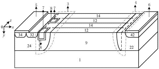
[0038] Such as figure 1 As shown, a high withstand voltage lateral superjunction device, its cell structure includes a second doping type substrate 1, a first doping type drift region 9, a second doping type strip 14, a first doping type strip 12. The first doping type source heavily doped region 32, the second doping type source heavily doped region 34, the second doping type well region 24, the first doping type well region 22, the second doping type well region Type multi-faceted depletion region 3, first doping type multi-faceted depletion region 4, first doping type drain heavily doped region 42, source contact electrode 5, drain contact electrode 6, polysilicon gate 7, gate oxide layer 8. In the first doping type drift region 9, the first doping type strips 12 and the second doping type strips 14 are alternately arranged along the Z positive direction, and at least one of the left surface and the right surface forms a multi-faceted depletion region , when the left surfa...
Embodiment 2
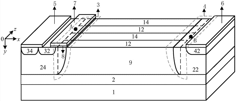
[0040] Such as figure 2 As shown, this embodiment is basically the same as Embodiment 1, the difference is that a buried oxide layer 2 is introduced between the second doped type substrate 1 and the first doped type drift region 9, and the upper surface of the buried oxide layer 2 is connected to the first doped type drift region 9. The lower surface of the drift region 9 of one doping type is connected, and the lower surface is connected with the upper surface of the substrate 1 of the second doping type.
[0041] Specifically, in the SOI cellular structure, the substrate 1 may be of the second doping type or the first doping type.
Embodiment 3
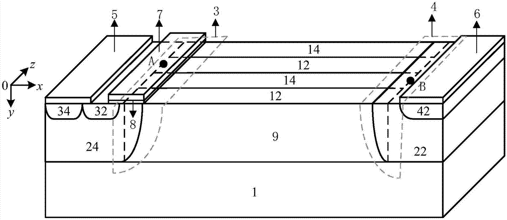
[0043] Such as image 3 As shown, this embodiment is basically the same as Embodiment 1, except that a second doping is provided between the substrate 1 of the second doping type, the well region 24 of the second doping type and the drift region 9 of the first doping type. Type buried layer 10. Lower the resistance at the bottom of the second doped well region to prevent the opening of the life-saving tube.
PUM
 Abstract
Description
Claims
Application Information
 - R&D
- Intellectual Property
- Life Sciences
- Materials
- Tech Scout
- Unparalleled Data Quality
- Higher Quality Content
- 60% Fewer Hallucinations
Browse by: Latest US Patents, China's latest patents, Technical Efficacy Thesaurus, Application Domain, Technology Topic, Popular Technical Reports.
© 2025 PatSnap. All rights reserved.Legal|Privacy policy|Modern Slavery Act Transparency Statement|Sitemap|About US| Contact US: help@patsnap.com