Manufacturing method for insulation structure of power electronic device

A technology of a power electronic device and a manufacturing method, which is applied in the field of the manufacture of an insulating structure, can solve the problems affecting the normal use of power electronic devices and the thermal conductivity of a copper substrate, and achieve the effect of increasing the thermal conductivity and ensuring the normal use.

Inactive Publication Date: 2017-11-03
QINGDAO JIAEN SEMICON
View PDF4 Cites 1 Cited by
  • Summary
  • Abstract
  • Description
  • Claims
  • Application Information

AI Technical Summary

Problems solved by technology

[0005] In the prior art, the method of insulating and protecting the copper substrate is usually to install an insulating layer on the side of the copper substrate facing the heat sink. The insulating layer can be a ceramic sheet or an insulating rubber sleeve. Although this method has played a certain role Insulation protection, but it has a great impact on the heat conduction of the copper substrate, affecting the normal use of power electronic devices

Method used


Image

  • Manufacturing method for insulation structure of power electronic device
  • Manufacturing method for insulation structure of power electronic device
  • Manufacturing method for insulation structure of power electronic device

Examples


Embodiment Construction

[0033] The following will clearly and completely describe the technical solutions in the embodiments of the present invention with reference to the accompanying drawings in the embodiments of the present invention. Obviously, the described embodiments are only some, not all, embodiments of the present invention. Based on the embodiments of the present invention, all other embodiments obtained by persons of ordinary skill in the art without making creative efforts belong to the protection scope of the present invention.

[0034] The embodiment of the invention discloses a method for manufacturing an insulating structure of a power electronic device.

[0035] figure 1 It is a structural schematic diagram of an insulating structure of a power electronic device according to an embodiment of the present invention, figure 2 for figure 1 For the cross-sectional schematic diagram of A-A, see figure 1 and figure 2 , an insulating structure of a power electronic device according t...


PUM


Abstract

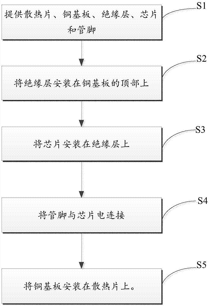
The invention discloses a manufacturing method for an insulation structure of a power electronic device, and belongs to the technical field of power electronics. The manufacturing method comprises the steps of providing a heat sink, a copper substrate, an insulation layer, a chip and pins; installing the insulation layer at a top part of the copper substrate; installing the chip on the insulation layer; electrically connecting the pins and the chip; and installing the copper substrate on a heat sink. According to the manufacturing method for the insulation structure of the power electronic device, the insulation layer is arranged on the copper substrate, thus, a current generated by the chip cannot be transferred to the copper substrate, the copper substrate is electrically insulated, and correspondingly, the insulation layer is unnecessary to arrange between the copper substrate and the heat sink. With the insulation structure of the power electronic device, manufactured by the method, the heat conduction effect of the copper substrate to the heat sink is better on the condition that the normal use function of the power electronic device is ensured, and the normal use of the power electronic device is more favorably ensured.

Description

technical field [0001] The invention belongs to the technical field of power electronics, and in particular relates to a method for manufacturing an insulating structure of a power electronic device. Background technique [0002] Copper substrate is the most expensive power electronic device among metal substrates. Its thermal conductivity is many times better than that of aluminum substrates and iron substrates. It is suitable for high-frequency circuits and areas with large changes in high and low temperature, as well as heat dissipation of precision communication equipment and architectural decoration industries. . [0003] The copper substrate is a conductive layer, and the copper substrate is usually mounted on a heat sink. In the application of many power electronic devices, the copper substrate needs to be insulated and protected. [0004] In the process of realizing the present invention, the applicant finds that there are at least the following deficiencies in the ...

Claims


Application Information

Patent Timeline
IPC IPC(8): H01L23/14H01L23/367
CPCH01L23/142H01L23/3672H01L2224/32245
Inventor 王丕龙徐旭王新强
Owner QINGDAO JIAEN SEMICON
Why Eureka
Try Eureka