A process control monitoring PCM device and monitoring method

A process control and device technology, which is applied in the field of process control monitoring PCM devices and monitoring, can solve the problems of complex operation, low efficiency and high cost, and achieve the effects of simple operation, improved efficiency and cost saving

Active Publication Date: 2019-10-15
FOUNDER MICROELECTRONICS INT
View PDF4 Cites 0 Cited by
  • Summary
  • Abstract
  • Description
  • Claims
  • Application Information

AI Technical Summary

Problems solved by technology

[0004] The purpose of the embodiments of the present invention is to provide a process control monitoring PCM device and monitoring method to solve the problem of using SEM to determine whether the hole is short-circuited with the polycrystal in the prior art. Not only is the operation complicated, but only 3 to 5 detections can be checked in one slice point, the efficiency is low, and the cost is high in large-scale operations

Method used


Image

  • A process control monitoring PCM device and monitoring method
  • A process control monitoring PCM device and monitoring method
  • A process control monitoring PCM device and monitoring method

Examples


Embodiment Construction

[0030] In order to make the technical problems, technical solutions and advantages to be solved by the present invention clearer, the following will describe in detail with reference to the drawings and specific embodiments.

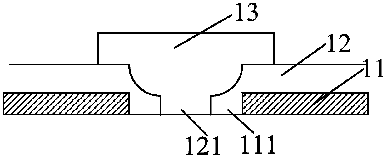
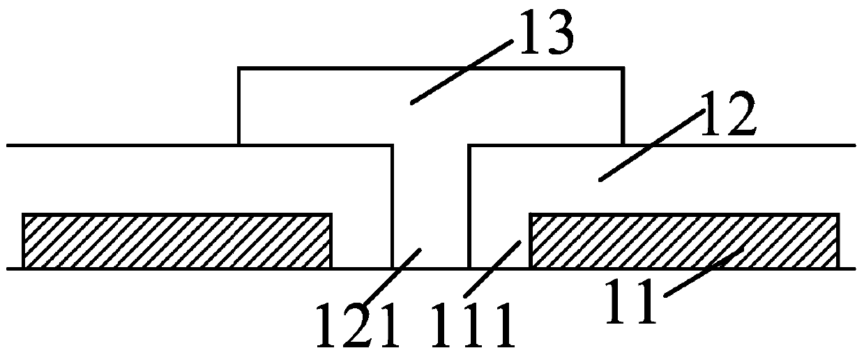
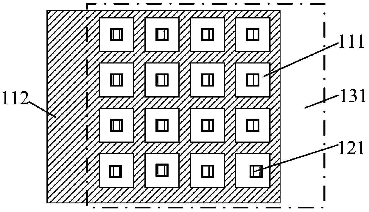
[0031] Such as Figure 1 to Figure 4 As shown, the process control monitoring PCM device of the embodiment of the present invention is applied to the short circuit detection between the via hole and the conductive layer in the chip to be tested according to predetermined design rules, wherein the process control monitoring PCM device includes:

[0032] One or more first via holes 111 and the first conductive layer 11 provided with the first lead-out 112 to be detected, the second conductive layer 13 provided with the second lead-out 131 to be detected, and the first The intermediate dielectric layer 12 between the conductive layer 11 and the second conductive layer 13, wherein the intermediate dielectric layer 12 is provided with a second via hole 121 co...


PUM


Abstract

The invention provides a process control monitor (PCM) device and a monitoring method, which are applied to short circuit detection between a via hole and a conductive layer in a to-be-detected chip which is fabricated in accordance with pre-designed rules. The PCM device includes: a first conductive layer which is provided with one or a plurality of via holes and a first leading-out terminal which is to be detected; a second conductive layer which is provided with a second leading-out terminal which is to be detected; an intermediate medium layer which is arranged between the first conductive layer and the second conductive layer, wherein the intermediate medium layer is perforated with second via holes which correspond to every first via hole, and the second conductive layer is arranged on the intermediate medium layer and fills the second via hole. The first conductive layer, the second conductive layer, the intermediate medium layer, the first via hole (s) and the second via hole are structured to conform to the pre-designed rules. The PCM device increases the efficiency in determining the presence of short circuit between the via holes and the first conductive layer, and saves cost.

Description

technical field [0001] The invention relates to the technical field of semiconductors, in particular to a process control monitoring PCM device and a monitoring method. Background technique [0002] The PCM (Process Control Monitor) test can directly reflect whether the manufacturing process of the chip is normal. Different PCM test devices can reflect different processes. The more reasonable the PCM device design is, the more accurate the feedback is whether the corresponding online process is normal. As the size of the semiconductor process becomes smaller and smaller, the size of the via hole used for metal connection is also smaller and smaller, and the abnormality of hole etching and hole photolithography will easily cause abnormal polycrystalline etching, which in turn will lead to the gap between the hole and the polycrystalline short circuit. [0003] The traditional method of using SEM (scanning electronic microscopy, scanning electron microscope) to judge whether...

Claims


Application Information

Patent Timeline
Patent Type & Authority Patents(China)
IPC IPC(8): H01L21/66
Inventor 杜蕾
Owner FOUNDER MICROELECTRONICS INT
Why Eureka
Try Eureka