
Patsnap Eureka
For R&D, Patsnap Eureka makes reading and utilizing patents & technical documents easy.
Patsnap Eureka AIR
Designed for self-driven R&D workflows. Generate viable solutions, solve complex R&D challenges, empower your innovation with AI.

Patsnap Eureka Materials
Designed for material experts only. Revolutionize your material R&D, from search, analyze, to developing new materials.

TechResearch
Generate reliable direction feasibility study reports for your R&D in just a few steps.

TechSeek
Discover and master advanced knowledge NOW. Basics, ideas, possibilities, all at once.

TechMind
As an expert in R&D Theories, TechMind can generates customized viable solutions instantly.

TechRisk
Analyze your overall solution with one click, know your potential R&D risks in advance.

TechMonitor
Get weekly tech updates, stay abreast of the latest tech innovations and key insights.
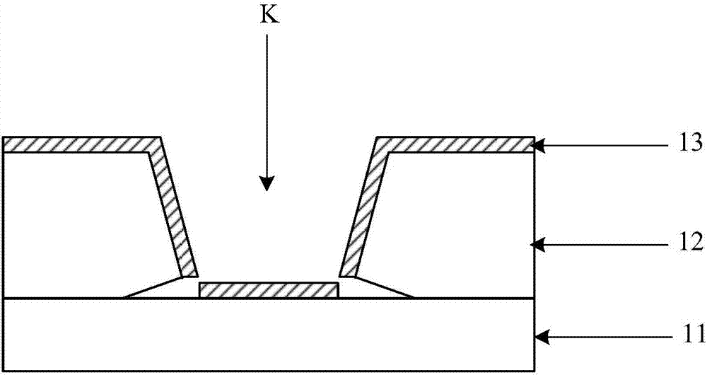
Display panel manufacturing method and display panel
A technology for display panels and manufacturing methods, applied to electrical components, electrical solid devices, circuits, etc., can solve problems such as easy fracture of pixel electrodes, and achieve the effect of stably forming electrical connections
- Summary
- Abstract
- Description
- Claims
- Application Information
AI Technical Summary
Problems solved by technology
Method used
Image

Examples
Embodiment Construction
[0069] In order to make the object, technical solution and advantages of the present invention clearer, the implementation manner of the present invention will be further described in detail below in conjunction with the accompanying drawings.
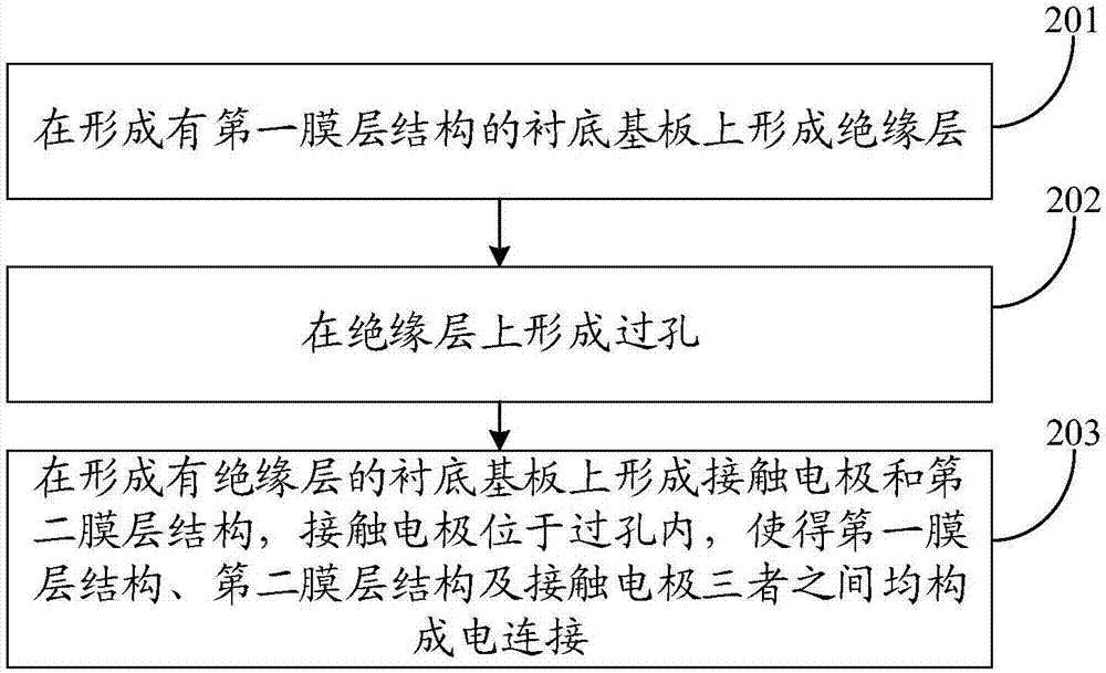
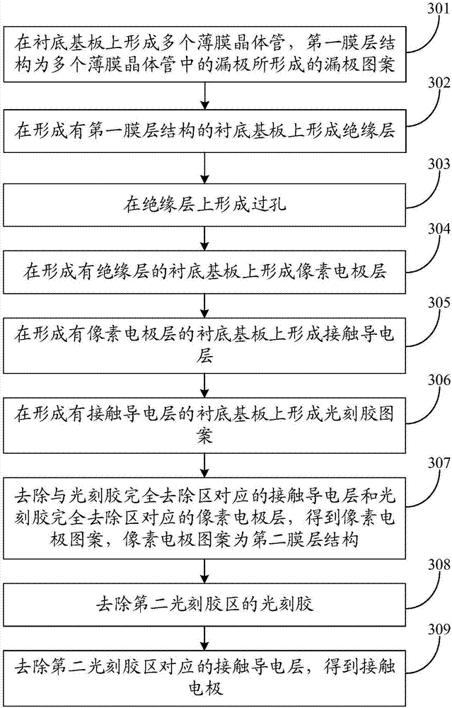
[0070] figure 2 It is a flow chart of a method for manufacturing a display panel shown in an embodiment of the present invention, and this embodiment is illustrated by taking the method for manufacturing a display panel as being applied to manufacturing a display panel. The manufacturing method of the display panel may include the following steps:
[0071] Step 201 , forming an insulating layer on the base substrate formed with the first film layer structure.
[0072] Step 202, forming a via hole on the insulating layer.
[0073] Step 203, forming a contact electrode and a second film layer structure on the base substrate formed with an insulating layer, the contact electrode is located in the via hole, so that the first film layer ...
PUM
 Abstract
Description
Claims
Application Information
 - R&D Engineer
- R&D Manager
- IP Professional
- Industry Leading Data Capabilities
- Powerful AI technology
- Patent DNA Extraction
Browse by: Latest US Patents, China's latest patents, Technical Efficacy Thesaurus, Application Domain, Technology Topic, Popular Technical Reports.
© 2024 PatSnap. All rights reserved.Legal|Privacy policy|Modern Slavery Act Transparency Statement|Sitemap|About US| Contact US: help@patsnap.com