Array substrate and display panel

A technology for array substrates and display areas, applied to static indicators, instruments, nonlinear optics, etc., to achieve the effect of protecting against short circuits

Active Publication Date: 2017-08-22
SHANGHAI TIANMA MICRO ELECTRONICS CO LTD
View PDF5 Cites 33 Cited by
  • Summary
  • Abstract
  • Description
  • Claims
  • Application Information

AI Technical Summary

Problems solved by technology

However, due to the increasing number of signal lines and consumers' demand for narrow bezels, there have been many problems in the design of ensuring a certain distance

Method used


Image

  • Array substrate and display panel
  • Array substrate and display panel
  • Array substrate and display panel

Examples


Embodiment Construction

[0023] An array substrate and a display panel of the present invention will be described in more detail below in conjunction with schematic diagrams, which represent a preferred embodiment of the present invention. It should be understood that those skilled in the art can modify the present invention described here and still realize the present invention. Favorable effect. Therefore, the following description should be understood as the broad knowledge of those skilled in the art, but not as a limitation of the present invention.

[0024] Terms used in the embodiments of the present invention are only for the purpose of describing specific embodiments, and are not intended to limit the present invention. As used in the embodiments of the present invention and the appended claims, the singular forms "a", "said" and "the" are also intended to include the plural forms unless the context clearly indicates otherwise.

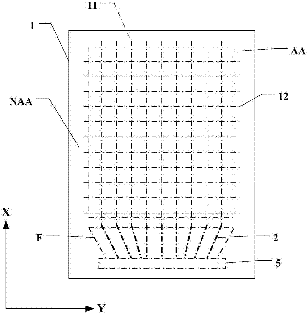
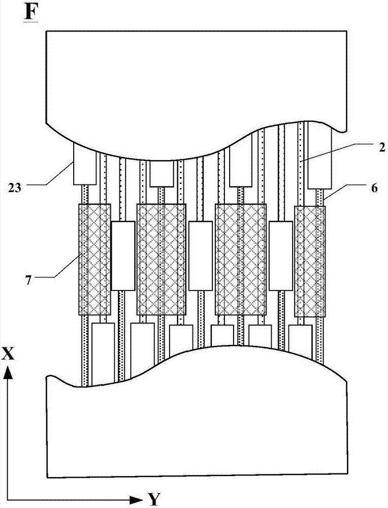
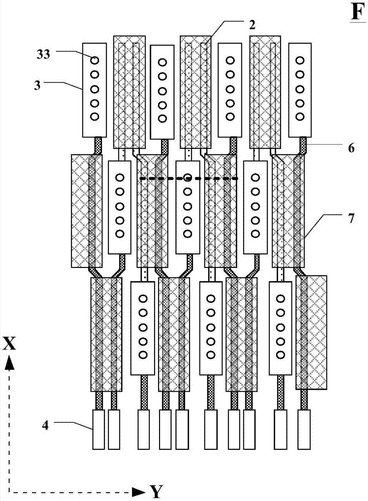
[0025] The present invention provides an array substrate, whic...


PUM


Abstract

The invention provides an array substrate. The array substrate has a display area and a non-display area surrounding the display area, and the display area is provided with gate lines and data lines; the array substrate further includes a fan-out area, at least one signal line and at least one binding terminal, wherein the fan-out area is arranged in the non-display area, the signal lines extend in the first direction, the first direction points to the fan-out area from the display area, the binding terminals are used for binding a drive circuit, the first terminal of each binding terminal is electrically connected with the corresponding signal line, and the second terminals of binding terminals are electrically connected with test terminals through first leading wires; the signal lines or the first leading wires are arranged among the binding terminals, the signal lines or the first leading wires in a region among the binding terminals are covered with a layer of covering electrodes, and the covering electrodes are electrically insulated with the signal lines or the first leading wires.

Description

technical field [0001] The present invention relates to the field of display technology, in particular to an array substrate and a display panel. Background technique [0002] At present, in the display panel, the driving circuit is electrically connected by binding the built-in driving pins with the binding terminals in the non-display area of ​​the display panel, that is, the pins and the binding terminals are in one-to-one correspondence to achieve pressing. [0003] Most of the binding terminals are located in the non-display area instead of the non-display area, and there are many related signal lines and dense wiring. In the process of bonding the drive circuit, due to the process deviation, the position of the bonding terminal and the pin of the drive circuit will fluctuate due to the deviation. In addition, if the wiring of the signal lines around the bonding terminal is relatively dense, the position of the pins of the drive circuit will coincide with the signal li...

Claims


Application Information

Patent Timeline
Patent Type & Authority Applications(China)
IPC IPC(8): G02F1/1345G09G3/00
CPCG02F1/13452G09G3/006G02F1/13456
Inventor 许作远朱桂熠
Owner SHANGHAI TIANMA MICRO ELECTRONICS CO LTD
Why Eureka
Try Eureka