
Method for error handling in a converter circuit for wiring of three voltage levels

A converter circuit, voltage level technology, applied in the output power conversion device, emergency protection circuit device, irreversible DC power input into AC power output and other directions, can solve the problem of power semiconductor switch aging, damage, power semiconductor Switch burden, etc.

Active Publication Date: 2007-05-23
ABB (SCHWEIZ) AG
View PDF2 Cites 8 Cited by
  • Summary
  • Abstract
  • Description
  • Claims
  • Application Information

AI Technical Summary

Problems solved by technology

[0005] A short circuit on all phases of the converter circuit of DE 699 02 227 T2 allows short circuit currents to be generated in the converter subsystem affected by the fault as well as in other converter subsystems, however, said short circuit currents burden the power semiconductor switches
A power semiconductor switch with such a burden would thus age faster or even be damaged, which means a severe impairment or in the worst case loss of the availability of the converter circuit

Method used


Image

  • Method for error handling in a converter circuit for wiring of three voltage levels
  • Method for error handling in a converter circuit for wiring of three voltage levels
  • Method for error handling in a converter circuit for wiring of three voltage levels

Examples


Embodiment Construction

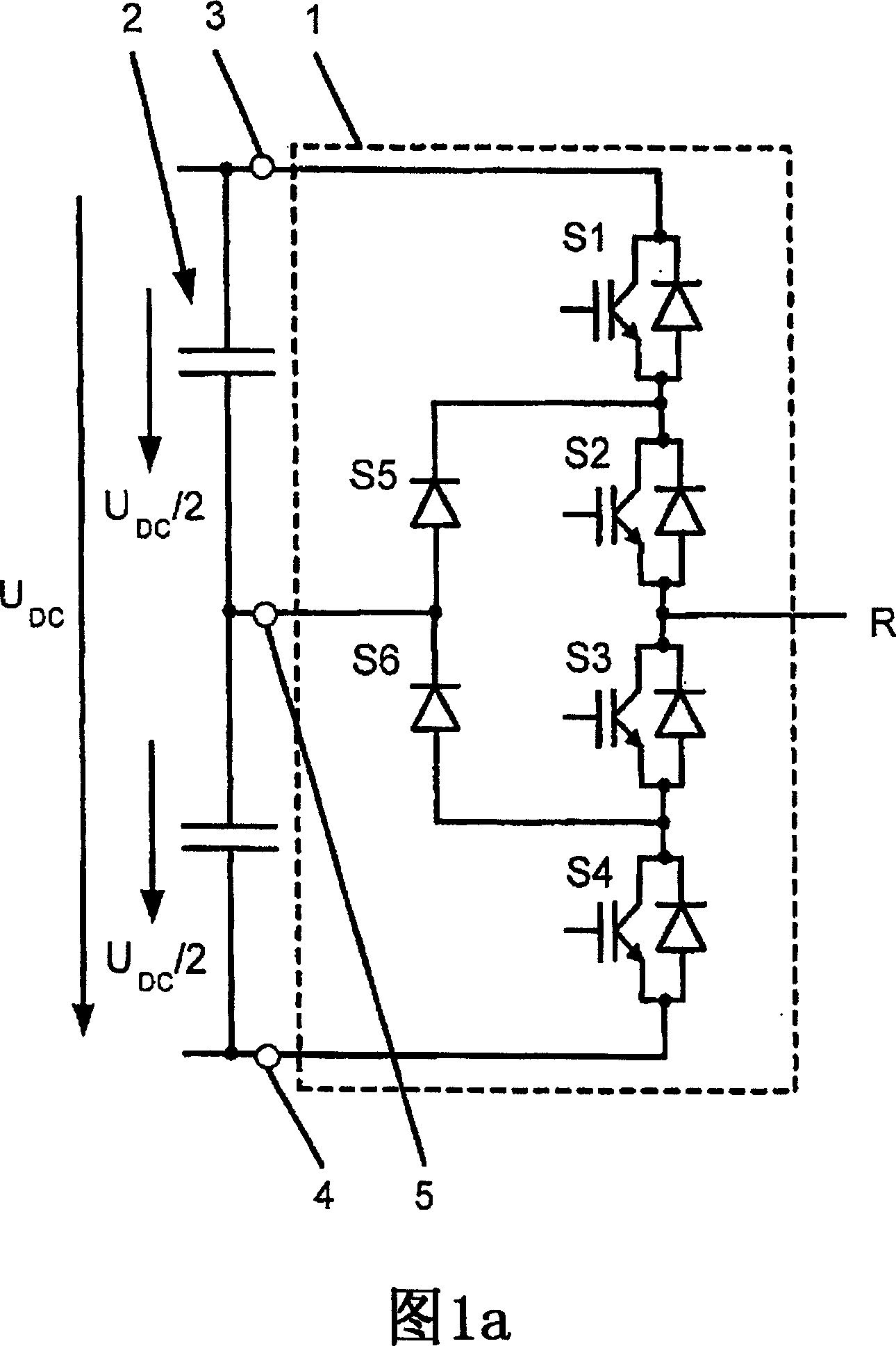
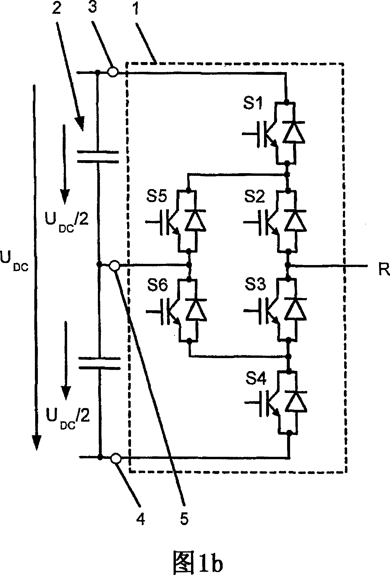
[0020]Figure 1a shows an embodiment of a known conventional converter subsystem 1 in a converter circuit for switching three voltage levels (already described in detail at the outset). The converter circuit has a converter subsystem 1 provided for each phase R, S, T, only one converter subsystem 1 for phase R is shown in FIG. 1a. The converter circuit comprises a DC voltage circuit 2 constituted by two capacitors connected in series, the first main connection 3 and the second main connection 4 and the secondary connection 5 of the DC voltage circuit 2 constituted by two adjacent and interconnected capacitors. In addition, the converter subsystem 1 has first, second, third and fourth actuatable bidirectional power semiconductor switches S1 , S2 , S3 , S4 and fifth and sixth power semiconductor switches S5 , S6 . In particular, each actuatable bidirectional power semiconductor switch S1 , S2 , S3 , S4 consists of an insulated gate bipolar transistor (IGBT) and a diode connected ...


PUM


Abstract

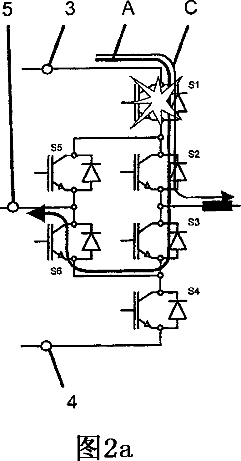
A method for error handling in a converter circuit for wiring of three voltage levels is disclosed, whereby the converter circuit comprises a partial converter system (1), for each phase (R, S, T), in which an upper error current path (A), or a lower error current path (B) is detected in the partial converter system (1). The upper error current path (A) runs over the first, second, third and sixth power semiconductor switch (S1, S2, S3, S6) of the partial converter system (1), or over the first and fifth power semiconductor switch (S1, S5) of the partial converter system (1) and the lower error current path (B) runs over the second, third, fourth and fifth power semiconductor switch (S2, S3, S4, S5) of the partial converter system (1) or over the fourth and sixth power semiconductor switch (S4, S6) of the partial converter system (1) and, after a error switching sequence the power semiconductor switches (S1, S2, S3, S4, S5, S6) are switched. According to the invention, a phase-side short-circuit of all phases of the converter circuit may be avoided and hence a secure operational state for the converter circuit in the case of an error may be achieved, whereby after the error switch sequence in the case of detection of the upper or the lower error current path (A, B), the switch status of each power semiconductor switch (S1, S2, S3, S4, S5, S6) on said detection is fixed. Furthermore, on detection of the upper error current path (A), the first power semiconductor switch (S1) and then the third power semiconductor (S3) are switched off and, on detection of the lower error current path (B), the fourth power semiconductor switch (S4) and then the second power semiconductor (S2) are switched off.

Description

technical field [0001] The invention relates to the field of start-up methods for converter circuits. The invention is based on a method for fault handling in a converter circuit switching three voltage levels according to the preamble of claim 1 . Background technique [0002] Power semiconductor switches are being used more and more in converter technology and in particular in converter circuits for switching three voltage levels. This converter circuit for switching three voltage levels is specified in DE 699 02 227 T2. FIG. 1 a shows a conventional converter subsystem for one phase of a converter circuit, wherein the converter subsystem shown in FIG. 1 a corresponds to that of DE 699 02 227 T2. As shown in Figure 1a, the converter circuit has a DC voltage circuit consisting of two capacitors connected in series, the first and second main and secondary connections of which are adjacent and interconnected by the two of capacitors. The capacitance values ​​of the two ca...

Claims


Application Information

Patent Timeline
Patent Type & Authority Applications(China)
IPC IPC(8): H02H7/122H02M7/48H02P27/06B60L3/00H02P27/14
CPCH02H7/1225H02M7/487H02M1/32H02M7/48
Inventor 格罗尔德·克纳普格哈德·霍赫施图尔鲁道夫·维泽尔勒克·迈森奇
Owner ABB (SCHWEIZ) AG
Learn More