display panel
A display panel and display medium layer technology, which is applied to housings with display/control units, instruments, printed circuits, etc., can solve the problem that conductive lines are difficult to meet the narrow frame design requirements, and achieve the effect of reducing the layout area
- Summary
- Abstract
- Description
- Claims
- Application Information
AI Technical Summary
Problems solved by technology
Method used
Image
Examples
Embodiment Construction
[0078] A number of embodiments of the present invention will be disclosed in the following figures. For the sake of clarity, many practical details will be described together in the following description. It should be understood, however, that these practical details should not be used to limit the invention. That is, in some embodiments of the present invention, these practical details are unnecessary. In addition, for the sake of simplifying the drawings, some existing conventional structures and elements will be shown in a simple and schematic manner in the drawings.
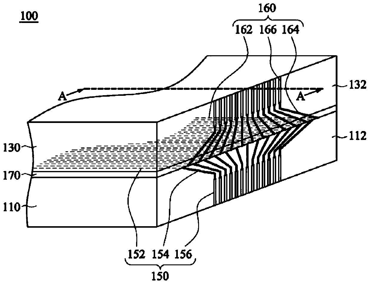
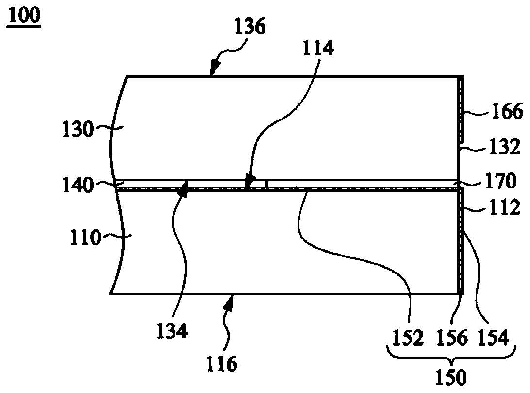
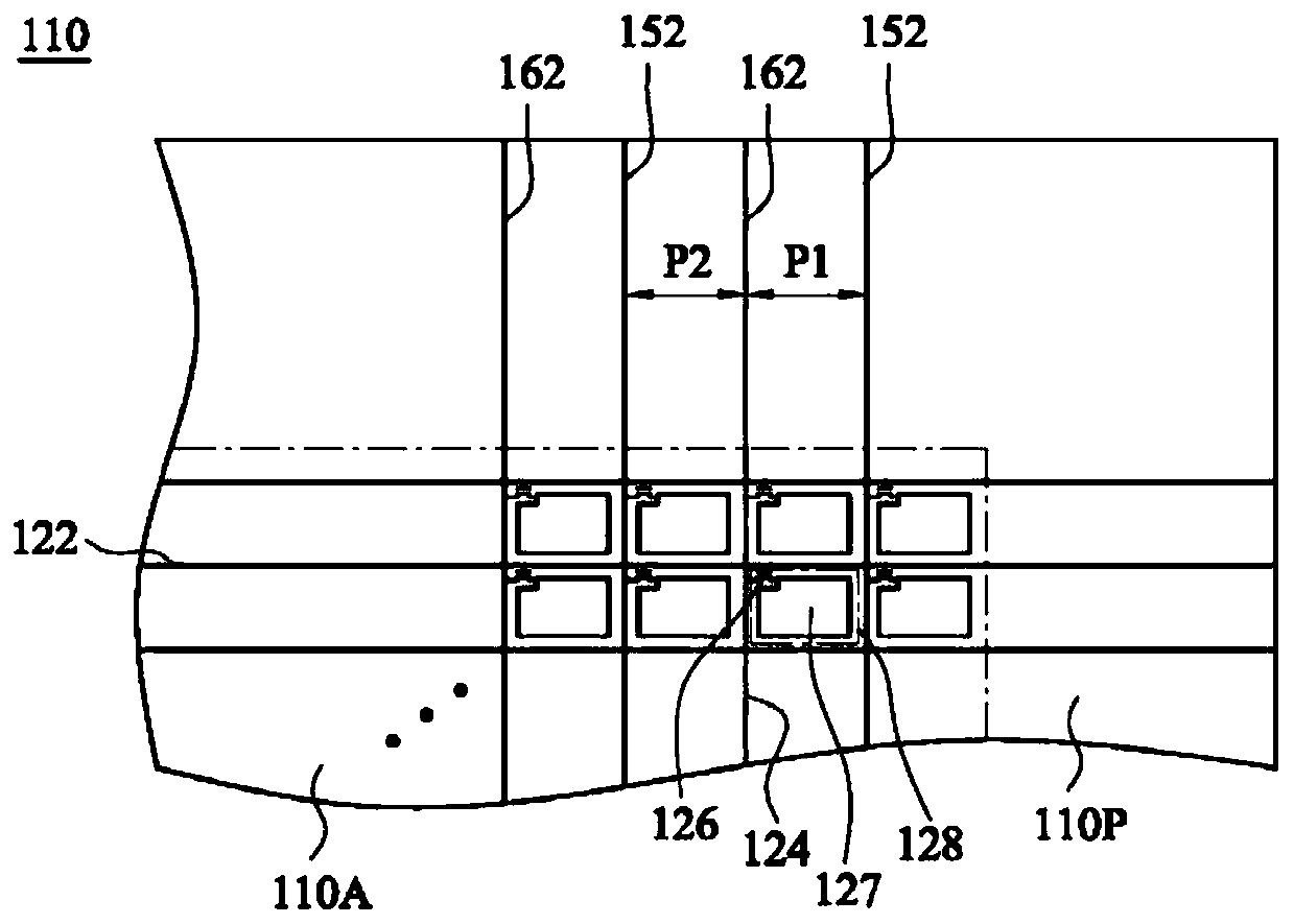
[0079] Figure 1A is a partial perspective view of a display panel 100 according to an embodiment of the present invention, Figure 1B is along Figure 1A The profile of the line segment A-A, while figure 2 yes Figure 1A A partial top view of the first substrate 110 of FIG. The display panel 100 includes a first substrate 110 , a second substrate 130 and a display medium layer 140 . The first substrate ...
PUM
 Abstract
Description
Claims
Application Information
 - R&D
- Intellectual Property
- Life Sciences
- Materials
- Tech Scout
- Unparalleled Data Quality
- Higher Quality Content
- 60% Fewer Hallucinations
Browse by: Latest US Patents, China's latest patents, Technical Efficacy Thesaurus, Application Domain, Technology Topic, Popular Technical Reports.
© 2025 PatSnap. All rights reserved.Legal|Privacy policy|Modern Slavery Act Transparency Statement|Sitemap|About US| Contact US: help@patsnap.com


