Fused quartz micro-hemispheric resonance gyroscope packaged based on SOI and processing method of fused quartz micro-hemispheric resonance gyroscope
A hemispherical resonant gyroscope and fused silica technology, applied in the fields of micro-electromechanical and inertial navigation, can solve the problems of increasing the cost and difficulty of MEMS packaging, and achieve the effects of simplifying the packaging process, enhancing the dynamic performance, and increasing the facing area.
- Summary
- Abstract
- Description
- Claims
- Application Information
AI Technical Summary
Problems solved by technology
Method used
Image
Examples
Embodiment 1
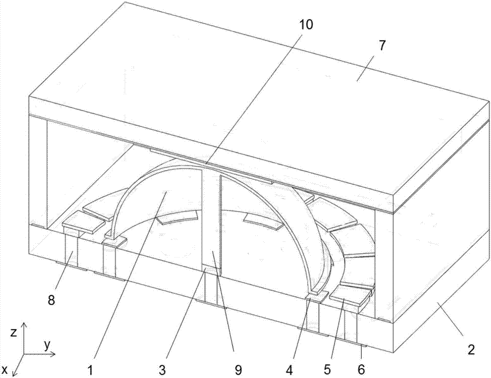
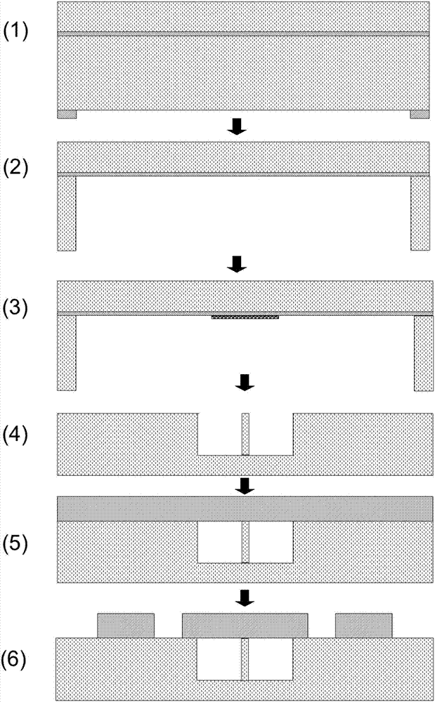
[0038] Such as Figure 1-3As shown, a fused silica microhemispherical resonator gyroscope based on SOI package, including glass substrate, SOI sealed shell, fused silica microhemispherical shell resonator, microhemispherical shell supporting column, reference electrode, 8 sensitive electrodes, 16 six Excitation electrodes, circular metal pads and cylindrical electrode through holes; the glass substrate is set at the bottom of the SOI sealed shell to form a closed cavity structure, the fused silica micro-hemispherical shell resonator is set at the center of the glass base, and the reference electrode is set at the fused The upper surface of the glass substrate at the center of the quartz micro-hemispherical shell resonator, the top of the micro-hemispherical shell support column is connected to the inner top surface of the hemisphere of the fused quartz micro-hemispherical shell resonator, and the bottom is connected to the reference electrode; 8 sensitive electrodes are evenly ...
Embodiment 2
[0054] It is basically the same as the embodiment 1, except that: the diameter of the hemispherical shell resonator is 2000 μm, and the thickness is 10 μm;
Embodiment 3
[0056] Basically the same as embodiment 1, the difference is: based on the processing method of the fused silica microhemispherical resonant gyroscope of SOI package, 8 sensitive electrodes in step (9) and 16 excitation electrodes in step (10) use silicon The wafer is processed and bonded so that it is respectively located on the upper surface of the glass substrate directly below the lip of the resonator of the micro-hemispherical shell and on the upper surface of the glass substrate outside the lip of the micro-hemispherical shell.
PUM
| Property | Measurement | Unit |
|---|---|---|
| diameter | aaaaa | aaaaa |
| thickness | aaaaa | aaaaa |
| diameter | aaaaa | aaaaa |
Abstract
Description
Claims
Application Information
 - R&D
- Intellectual Property
- Life Sciences
- Materials
- Tech Scout
- Unparalleled Data Quality
- Higher Quality Content
- 60% Fewer Hallucinations
Browse by: Latest US Patents, China's latest patents, Technical Efficacy Thesaurus, Application Domain, Technology Topic, Popular Technical Reports.
© 2025 PatSnap. All rights reserved.Legal|Privacy policy|Modern Slavery Act Transparency Statement|Sitemap|About US| Contact US: help@patsnap.com


