
Switch power supply circuit and adjusting method thereof

A technology of switching power supply circuit and adjustment method, applied in the direction of electrical components, output power conversion devices, etc., can solve the problems of difficulty in accommodating buffer circuits, tight layout of PCB boards, etc., and achieve the effect of saving layout area and reducing the number of components

Active Publication Date: 2017-07-14
KUSN INFOVISION OPTOELECTRONICS
View PDF3 Cites 14 Cited by
  • Summary
  • Abstract
  • Description
  • Claims
  • Application Information

AI Technical Summary

Problems solved by technology

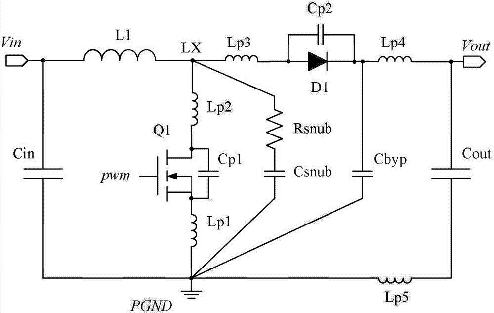
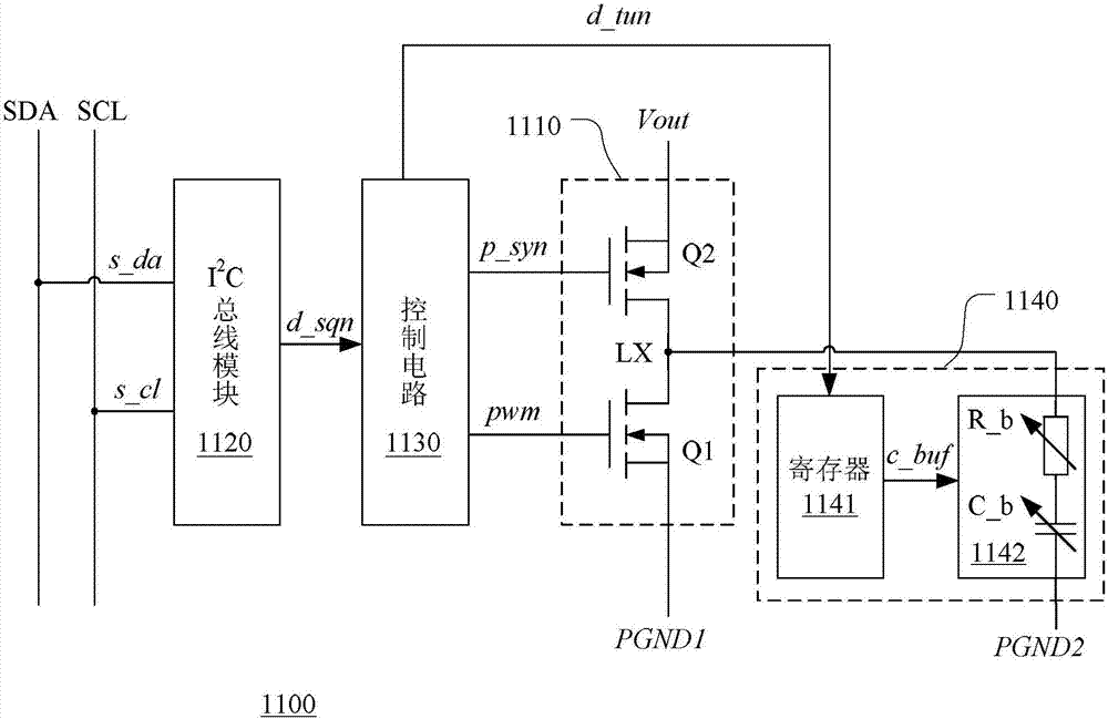
[0009] In order to solve the above-mentioned problems in the prior art, the object of the present invention is to provide a switching power supply circuit and its adjustment method, which solves the problem in the prior art that the signal integrity at the switch node can only be adjusted by manually replacing capacitors and resistors. problem and the tight layout on the PCB makes it difficult to accommodate snubber circuits

Method used


Image

  • Switch power supply circuit and adjusting method thereof
  • Switch power supply circuit and adjusting method thereof
  • Switch power supply circuit and adjusting method thereof

Examples


Embodiment Construction

[0027] Hereinafter, the present invention will be described in more detail with reference to the accompanying drawings. In the various figures, identical elements are indicated with similar reference numerals. For the sake of clarity, various parts in the drawings have not been drawn to scale. Also, some well-known parts may not be shown in the drawings.

[0028] In the following, many specific details of the present invention are described, such as device structures, materials, dimensions, processing techniques and techniques, for a clearer understanding of the present invention. However, the invention may be practiced without these specific details, as will be understood by those skilled in the art.

[0029] The power management unit of the first embodiment of the present invention includes at least one switching power supply circuit.

[0030]The switching power supply circuit can be a step-up structure (Boost), a step-down structure (Buck), or a step-down structure (Boos...


PUM


Abstract

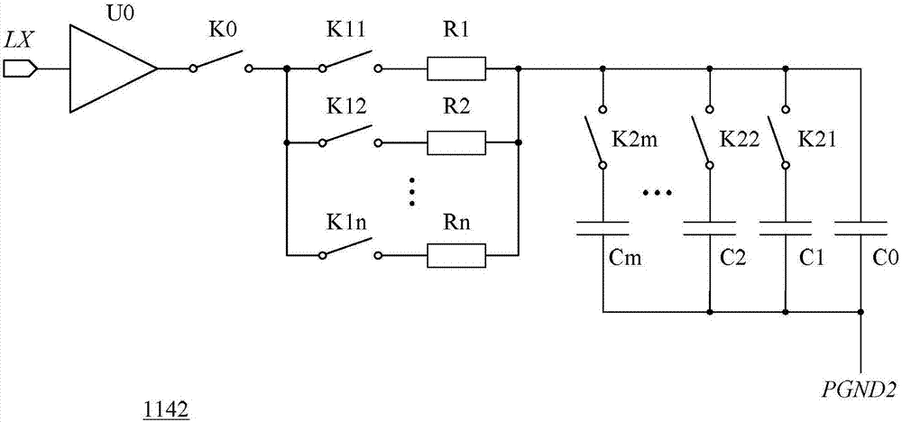
The invention discloses a switch power supply circuit and an adjusting method thereof. The switch power supply circuit comprises a main circuit, an I<2>C bus module, a control circuit, and a buffer circuit; the main circuit comprises a switch node and a main switch tube controlled by a switch signal, and the main circuit comprises a first grounding end, an input end for receiving an input DC signal, and an output end for providing an output DC signal; the I<2>C bus module generates control data; the control circuit generates the switch signal according to the control data and / or the output DC signal, and generates an adjustment data signal according to the control data; and the buffer circuit is connected between a second grounding end and the switch node of the main circuit, and resistance and capacitance values of the buffer circuit are controlled by the adjustment data signal, so repeated welding and removal do not need to be performed on the buffer circuit, a buffer grounding path matching the main circuit of the switch power supply circuit is provided at a position of the switch node then, and signal waveform integrity and debugging efficiency at the position of the switch node are improved.

Description

technical field [0001] The present invention relates to the field of electronic circuits, and more specifically, to a switching power supply circuit and an adjusting method thereof. Background technique [0002] The switching power supply circuit has the advantages of high efficiency and large output current, so it is widely used in circuits in various fields, for example, the switching power supply circuit is designed in the backlight driver chip as the power supply module of the display backlight module, and the switching power It is used in the bias power drive chip in the liquid crystal display module (LCD Module, LCM), and the switching power supply circuit is designed in the charging chip to realize charging the battery, etc. [0003] However, the switching power supply circuit often causes ringing at the switching node due to the influence of parasitic capacitance and parasitic inductance, which will affect the integrity of the signal and may be affected by electromag...

Claims


Application Information

Patent Timeline
Patent Type & Authority Applications(China)
IPC IPC(8): H02M1/34
CPCH02M1/34
Inventor 吴春芸双强张春宇
Owner KUSN INFOVISION OPTOELECTRONICS
Learn More