
Semiconductor device, control method and converter

A technology of semiconductors and converters, applied in the electronic field, can solve the problems of poor reverse recovery characteristics of body diodes, low switching frequency, and large switching losses

Active Publication Date: 2017-07-07
HUAWEI DIGITAL POWER TECH CO LTD
View PDF6 Cites 12 Cited by
  • Summary
  • Abstract
  • Description
  • Claims
  • Application Information

AI Technical Summary

Problems solved by technology

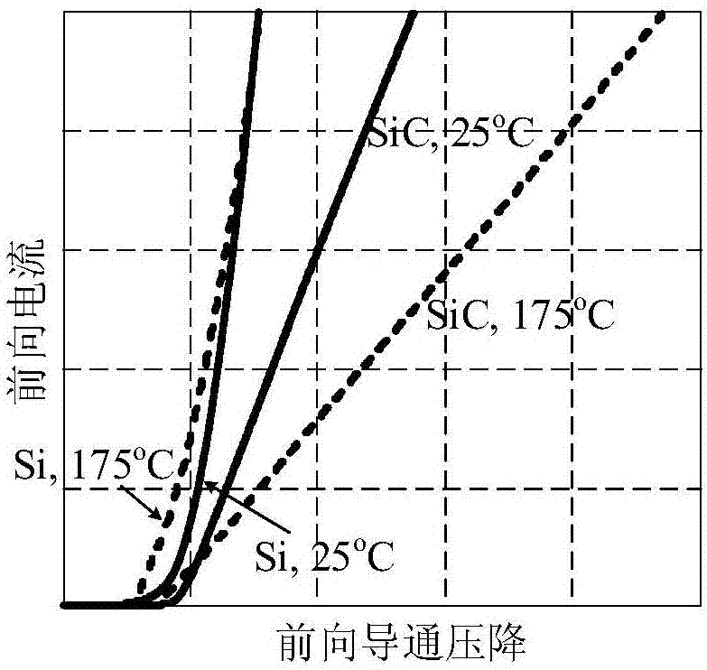
[0006] To sum up, Schottky diodes made of wide bandgap materials have no reverse recovery current, but the forward conduction voltage drop is large and the cost is high, which is not conducive to reducing the conduction loss and cost of the converter
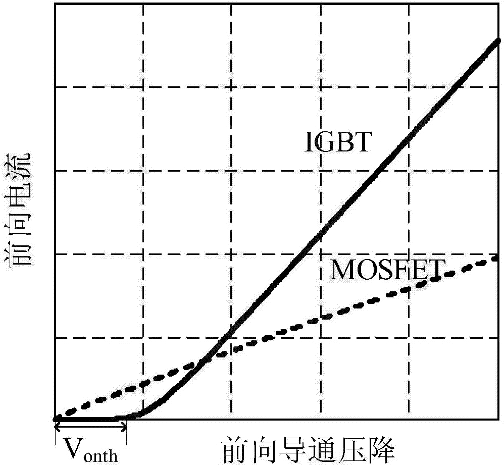
The switching frequency of MOSFET is high, but the current capacity is low, the reverse recovery characteristics of body diode are poor, and the conduction voltage of IGBT is reduced, but the switching loss is large, and the switching frequency is low. Single use or simple parallel connection cannot combine the advantages of each device and reduce the transformation. Converter loss, improve converter performance

Method used


Image

  • Semiconductor device, control method and converter
  • Semiconductor device, control method and converter
  • Semiconductor device, control method and converter

Examples


Embodiment Construction

[0075] The terms "first", "second" and the like in the specification and claims of the present application and the above drawings are used to distinguish similar objects, and are not necessarily used to describe a specific sequence or sequence. It is to be understood that the terms so used are interchangeable under appropriate circumstances such that the embodiments described herein can be practiced in sequences other than those illustrated or described herein. Furthermore, the terms "comprising" and "having", as well as any variations thereof, are intended to cover a non-exclusive inclusion, for example, a process, method, system, product or device comprising a sequence of steps or elements is not necessarily limited to the expressly listed instead, may include other steps or elements not explicitly listed or inherent to the process, method, product or apparatus.

[0076] The technical solutions in the embodiments of the present application are described below with reference ...


PUM


Abstract

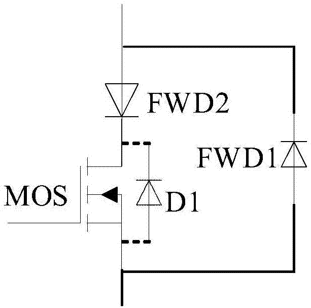
The embodiment of the invention discloses a semiconductor device and a converter. The semiconductor device provided by the invention comprises a low-voltage switch device, a first diode and a second diode, wherein the low-voltage switch device and the first diode form a series structure, the second diode is connected in parallel with two ends of the series structure formed by the low-voltage switch device and the first diode, the current passing directions of the first diode and the second diode are consistent, the first diode is a low-conduction voltage drop diode, and the second diode is a low-reverse recovery diode. When the semiconductor device is in a conduction state, control equipment controls the low-voltage switch device to be conducted, and simultaneous follow current is performed by the first diode and the second diode to reduce conduction voltage drop of the semiconductor device; and when the semiconductor device is switched off, the control equipment controls the low-voltage switch device to be switched off in advance of preset time, so that a load current is completely transferred to the second diode, and current exchange is achieved by the second diode and a complementary device to reduce a reverse recovery current of the semiconductor device.

Description

technical field [0001] The invention relates to the field of electronic technology, in particular to a semiconductor device, a control method and a converter. Background technique [0002] As the core link of electric energy conversion, the converter is widely used in various electrical equipment to realize alternating current (English: Alternating Current, abbreviation: AC) / direct current (English: Direct Current, abbreviation: DC), AC / AC, DC / Energy conversion between DC and DC / AC. In order to improve the power density of the converter and reduce the weight and volume of the equipment, Metal-Oxide Semiconductor Field-Effect Transistor (English: Metal-Oxide Semiconductor Field-Effect Transistor, referred to as: MOSFET) and insulated gate bipolar transistor (English: Insulated Gate Bipolar Transistor) Gate Bipolar Transistor, referred to as: IGBT) is widely used in converters due to its high switching frequency and low switching loss. [0003] In the converter, the diode u...

Claims


Application Information

Patent Timeline
IPC IPC(8): H02M1/088H03K17/567
CPCH02M1/088H03K17/567H03K2217/0036
Inventor 王朝辉石磊傅电波
Owner HUAWEI DIGITAL POWER TECH CO LTD
Learn More