Silicon chip correcting equipment

A technology of equipment and silicon wafers, applied in electrical components, conveyor objects, transportation and packaging, etc., can solve the problems of scrapping silicon wafers, increasing production costs, and chipping of silicon wafers, and achieves the effect of high correction efficiency.

Pending Publication Date: 2017-06-27
EGING PHOTOVOLTAIC TECHNOLOGY CO LTD
View PDF5 Cites 1 Cited by
  • Summary
  • Abstract
  • Description
  • Claims
  • Application Information

AI Technical Summary

Problems solved by technology

[0003] The technical problem to be solved by the present invention is: in order to solve the problem that the traditional correcting equipment is to change the position of the silicon wafer through contact with both sides of the silicon wafer. Since the silicon wafer itself is relatively brittle and fragile, it is easy to pinch the silicon wafer, resulting in Silicon wafers are scrapped and the production cost is increased. Now a silicon wafer correction equipment is provided.

Method used


Image

  • Silicon chip correcting equipment
  • Silicon chip correcting equipment
  • Silicon chip correcting equipment

Examples


Embodiment

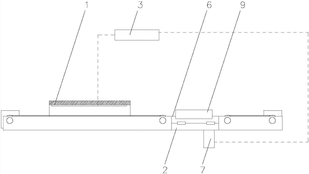
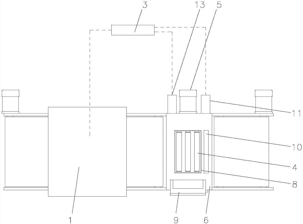
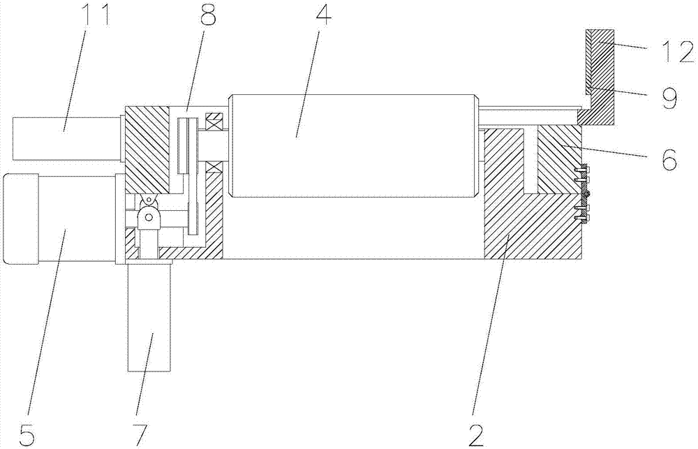
[0016] Such as Figure 1-3 As shown, a silicon wafer straightening device includes a detection device 1, a frame 2 and a control unit 3, the frame 2 is provided with a roller shaft 4 for rotation, and the frame 2 is provided with a roller shaft for driving the roller shaft 4 to rotate The motor 5, the frame 2 is provided with a substrate 6 for rotation, the frame 2 is provided with a first driving device 7 for driving the substrate 6 to rotate, the substrate 6 is provided with a groove 8, and the roller The shaft 4 is located in the groove 8, the base plate 6 is slidably provided with a limit plate 9 at one end of the axis direction of the roller shaft 4, and the frame 2 is provided with a second driving device 13 for driving the limit plate 9 to slide. , the base plate 6 is provided with a partition 10, the partition 10 is located at the output end of the roller shaft 4, and the base is provided with a third driving device 11 for driving the partition 10 to rise or fall, so ...


PUM


Abstract

The invention relates to the technical field of silicon chip production equipment, in particular to silicon chip correcting equipment. The silicon chip correcting equipment comprises a detecting device, a frame and a control unit; a roller shaft is rotationally arranged on the frame; the frame is provided with a motor for driving the roller shaft to rotate, is rotationally provided with a substrate, and is provided with a first driving device for driving the substrate to rotate; the substrate is provided with a groove; and the roller shaft is positioned in the groove. When the silicon chip correcting equipment is used, through rotation of the substrate, the conveying of silicon chips is stopped by a separation wall, so that the silicon chips are contacted with a limiting plate under the effect of self weights for correction; and then, the substrate rotates to recover an original state, and the silicon chips are output, so that the correcting efficiency is high, the position change of the silicon chips due to contact with two sides of the silicon chips in traditional correcting equipment is prevented, and the problems of increment of the production cost and wastes of the silicon chips due to easier clamping damage of the silicon chips caused by more brittle and fragile silicon chips are prevented.

Description

technical field [0001] The invention relates to the technical field of silicon wafer production equipment, in particular to a silicon wafer rectification equipment. Background technique [0002] In the photovoltaic cutting process, the cut silicon wafers need to be placed in flower baskets or inspected by a sorting machine one by one. Generally, these two processes are carried out on the conveyor belt, and both involve the position correction of the silicon wafers. Traditional correction equipment changes the position of the silicon wafer by contacting both sides of the silicon wafer. Since the silicon wafer itself is relatively brittle and fragile, it is easy to pinch the silicon wafer, resulting in the scrapping of the silicon wafer and increasing production costs. Contents of the invention [0003] The technical problem to be solved by the present invention is: in order to solve the problem that the traditional correcting equipment is to change the position of the silic...

Claims


Application Information

Patent Timeline
IPC IPC(8): B65G47/24H01L21/677
CPCH01L21/677B65G47/24
Inventor 孙铁囤汤平姚伟忠
Owner EGING PHOTOVOLTAIC TECHNOLOGY CO LTD
Why Eureka
Try Eureka