Ultra-wide bandwidth pulse generation circuit

An ultra-wideband pulse and circuit-generating technology, applied in the field of communications, can solve the problems that the pulse waveform is not suitable for antenna transmission, increase the circuit complexity and cost, and the ultra-wideband pulse technology is complicated.

Pending Publication Date: 2017-06-13
NANJING UNIV OF POSTS & TELECOMM
View PDF4 Cites 4 Cited by
  • Summary
  • Abstract
  • Description
  • Claims
  • Application Information

AI Technical Summary

Problems solved by technology

However, the existing pulse generation circuit based on avalanche triode requires high power supply voltage, which is not conducive to the miniaturization and mobile portability of the equipment, and the general pulse generation circuit based on avalanche triode can only directly generate Gaussian pulse, and Gaussian pulse contains DC components and more low-frequency components are not suitable for antenna transmission, so it is necessary to add an additional pulse shaping circuit to differentiate and filter the generated Gaussian pulses to obtain high-order Gaussian pulses or other waveforms suitable for antenna transmission, and the traditional pulse The power of the generating circuit is small, the generated pulse amplitude is low, and it is often necessary to add an additional broadband amplifier, which increases the complexity and cost of the circuit
[0005] In summary, the existing ultra-wideband pulse technology is complicated, the pulse amplitude is low, and the pulse waveform is not suitable for the transmission of the antenna

Method used


Image

  • Ultra-wide bandwidth pulse generation circuit
  • Ultra-wide bandwidth pulse generation circuit
  • Ultra-wide bandwidth pulse generation circuit

Examples


Embodiment Construction

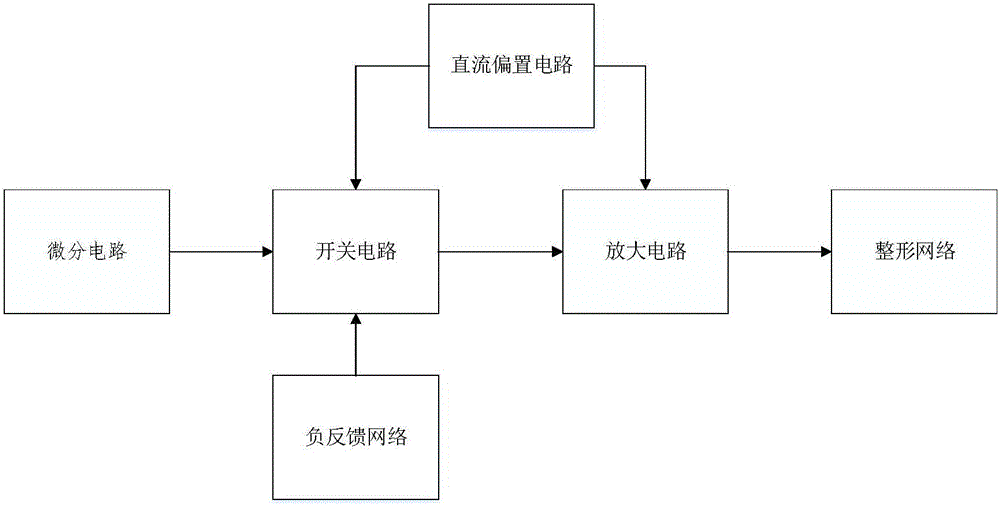
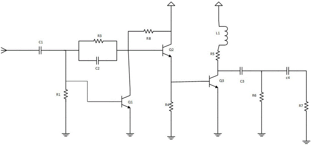
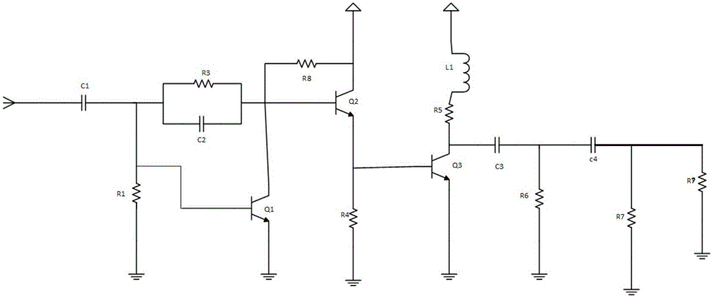
[0029] In order to further illustrate the technical means adopted by the present invention and the achieved effects, the technical solutions of the present invention will be clearly and completely described below in conjunction with the accompanying drawings and specific embodiments. Such as figure 1 The entire ultra-wideband pulse includes five parts: switch circuit, amplifier circuit, differential circuit, DC bias module, negative feedback network, and shaping network.

[0030] The differential circuit, switch circuit, amplifying circuit, and shaping network are connected in sequence, and the DC bias module provides DC bias for the switch circuit and the amplifying circuit.

[0031]The first differential circuit is composed of C1 and R1, which is connected to the external input crystal oscillator to extract the edge of the external crystal oscillator input signal; the negative feedback network is composed of C2 and R3, which greatly reduces the influence of the stability of ...


PUM


Abstract

The invention mainly relates to an ultra-wide bandwidth pulse generation circuit, comprising a differentiating circuit, a negative feedback network, a direct current bias module, a switch circuit, an amplifier circuit and a shaping network. The differentiating circuit is connected with an external digital signal. The amplifier circuit is connected with the switch circuit, thereby amplifying the amplitude of a pulse signal. The two-level differentiating circuits of the shaping network shape the amplified pulse signal into a nanosecond level ultra-wide bandwidth pulse signal. According to the switch circuit, a switch controlled square wave signal is generated through utilization of a switch characteristic of a triode. According to the amplifier circuit, the generated square wave signal with the relatively high amplitude is amplified through the triode and an energy storage inductor, so the amplitude of an output waveform is relatively high. According to the shaping circuit, the pulse signal with the relatively high amplitude is shaped into the nanosecond level ultra-wide bandwidth pulse signal through the two-level differentiating circuits. According to the scheme, the ultra-wide bandwidth pulse signal without a direct current component is generated, the signal is applied to antenna transmission, and the complexity of the whole circuit is reduced.

Description

technical field [0001] The invention relates to the communication field, and is particularly widely used in ground penetrating radar and communication. [0002] technical background [0003] UWB (Ultra-wide Bandwidth) is a carrier-free communication technology that uses nanosecond (ns) to picosecond (ps) level non-sine wave narrow pulses to transmit data, and time modulation technology can greatly increase its transmission speed. Moreover, the power consumption is relatively low, and it has a more accurate positioning capability. Different from the continuous carrier method used in common communications, UWB uses extremely short pulse signals to transmit data. The bandwidth occupied by these pulses even reaches several GHz, so the maximum data transmission rate can reach hundreds of Mb / ps. Because of the use of extremely short pulses, while communicating at high speed, the transmission power of UWB equipment is very small, only a few hundredths of the current continuous car...

Claims


Application Information

Patent Timeline
IPC IPC(8): H03K5/156
CPCH03K5/156
Inventor 肖建王吉石国伟程景清蔡志匡郭宇锋
Owner NANJING UNIV OF POSTS & TELECOMM
Why Eureka
Try Eureka