OLED packaging method and OLED packaging structure

A packaging method and packaging structure technology, applied in the direction of semiconductor devices, electrical components, circuits, etc., can solve the problems of accelerated aging of OLED devices, life decay of OLED devices, and prone to defects, so as to improve the quality of light emission and service life, and improve packaging Effect, effect of blocking invasion

Active Publication Date: 2019-01-22
TCL CHINA STAR OPTOELECTRONICS TECH CO LTD
View PDF1 Cites 0 Cited by
  • Summary
  • Abstract
  • Description
  • Claims
  • Application Information

AI Technical Summary

Problems solved by technology

[0006] However, as the OLED device is energized and operated, the encapsulation glue around the OLED device is gradually aging, and defect points are prone to appear, resulting in the opportunity for water and oxygen to infiltrate, thereby accelerating the aging of the OLED device and greatly reducing the life of the OLED device.

Method used


Image

  • OLED packaging method and OLED packaging structure
  • OLED packaging method and OLED packaging structure
  • OLED packaging method and OLED packaging structure

Examples


Embodiment Construction

[0050] In order to further explain the technical means adopted by the present invention and its effects, the following describes in detail the preferred embodiments of the present invention and the accompanying drawings.

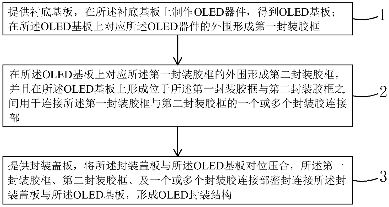
[0051] See image 3 , The present invention first provides the first OLED packaging method, including the following steps:

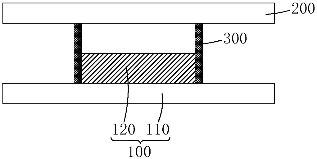
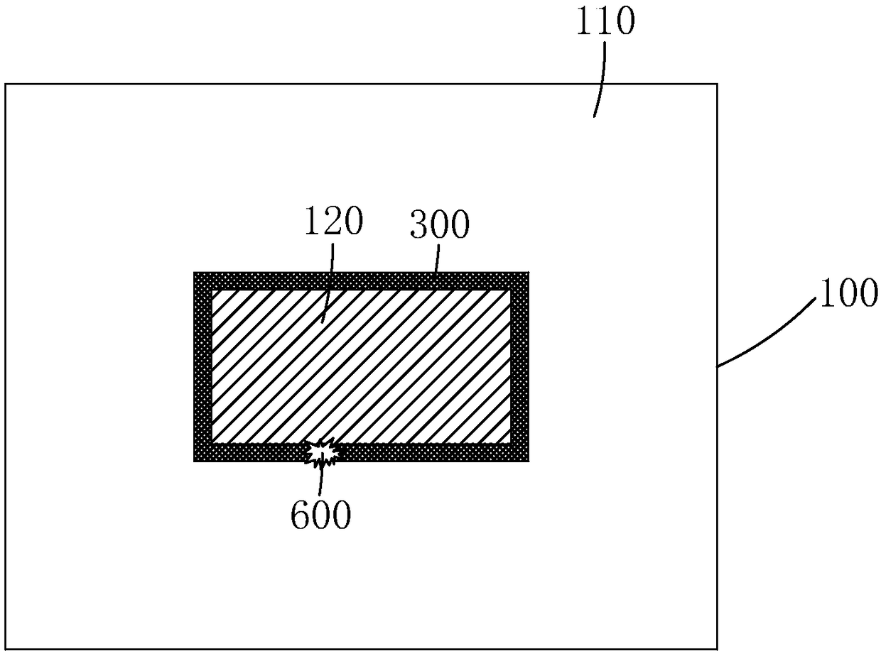
[0052] Step 1, such as Figure 4 As shown, a base substrate 11 is provided, and an OLED device 12 is fabricated on the base substrate 11 to obtain an OLED substrate 10;

[0053] A first encapsulating frame 31 is formed on the OLED substrate 10 corresponding to the periphery of the OLED device 12.

[0054] Specifically, in the step 1, the OLED device 12 is fabricated on the base substrate 11 by an evaporation method.

[0055] Step 2, such as Figure 5 As shown, a second encapsulation frame 32 is formed on the OLED substrate 10 corresponding to the periphery of the first encapsulation frame 31, and a second encapsulation frame 32 is formed on the ...


PUM


Abstract

The present invention provides an OLED encapsulation method and an OLED encapsulation structure. By arranging at least two encapsulation plastic frames around the OLED device, the probability of infiltration of water and oxygen from the outside can be significantly reduced. It will affect the internal OLED device; further, by setting one or more encapsulation joints between two adjacent encapsulation frames, multiple different encapsulation frames can be formed between two adjacent encapsulation frames Continuous sealing space, so as to effectively block the flow of water and oxygen between different sealing spaces, so that any defect point on any packaging plastic frame may only affect the sealing space where it is located, and will not affect other sealing spaces , to further block the invasion of external water and oxygen to the OLED device, and improve the packaging effect of the OLED device; based on the above two technical features, the present invention solves the problem of water and oxygen infiltration caused by the aging of the packaging plastic frame, and significantly improves the OLED device. Luminous quality and service life.

Description

Technical field [0001] The invention relates to the field of display technology, in particular to an OLED packaging method and an OLED packaging structure. Background technique [0002] Organic Light Emitting Display (OLED) has self-luminescence, low driving voltage, high luminous efficiency, short response time, high definition and contrast, nearly 180° viewing angle, wide operating temperature range, and can realize flexible display and Large-area full-color display and many other advantages are recognized by the industry as the display device with the most potential for development. [0003] According to the driving mode, OLED can be divided into passive matrix OLED (Passive Matrix OLED, PMOLED) and active matrix OLED (Active Matrix OLED, AMOLED), namely direct addressing and thin film transistor matrix addressing. Among them, AMOLED has pixels arranged in an array, is an active display type, has high luminous efficiency, and is usually used as a high-definition large-size disp...

Claims


Application Information

Patent Timeline
Patent Type & Authority Patents(China)
IPC IPC(8): H01L51/52H01L51/56
CPCH10K50/841H10K50/8426H10K71/00H10K59/875
Inventor 匡友元
Owner TCL CHINA STAR OPTOELECTRONICS TECH CO LTD
Why Eureka
Try Eureka