Planar diode

A diode and planar technology, applied in the field of planar diodes, can solve the problems of unreasonable structure design of diodes, unsuitable for large-scale production, etc., and achieve the effects of reasonable structure design, cost-effective production and good use effect.

Inactive Publication Date: 2017-06-09
夏振宇
View PDF0 Cites 0 Cited by
  • Summary
  • Abstract
  • Description
  • Claims
  • Application Information

AI Technical Summary

Problems solved by technology

The existing diode structure design is unreasonable and not suitable for industrialized mass production

Method used


Image

  • Planar diode

Examples


Embodiment Construction

[0010] The present invention will be further explained below in conjunction with the accompanying drawings and embodiments.

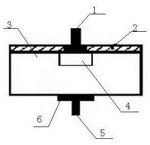
[0011] like figure 1 As shown, a planar diode includes an anode lead 1 and a silicon dioxide layer 2. The N-type silicon layer 3 is compatible with the silicon dioxide 2 layer. The N-type silicon layer 3 is covered with a P-type silicon chip 4. One side of the N-type silicon wafer 4 is adapted to the silicon dioxide layer 2, and one side of the N-type silicon layer 3 is provided with a negative electrode lead 5. One end of the positive electrode lead 1 or the negative electrode lead 5 is provided with a joint 6 .

[0012] The above content is an example and description of the present invention, but it does not mean that the advantages that the present invention can obtain are limited by this, and any simple transformation of the structure that may be possible in the practice of the present invention, and / or one of the advantages realized in some embodi...


PUM


Abstract

The invention discloses a planar diode, which comprises an anode lead (1) and a silicon dioxide layer (2), the N-type silicon layer (3) is compatible with the silicon dioxide (2) layer, and the N-type silicon layer (3) Covered with a P-type silicon chip (4), one side of the P-type silicon chip (4) is adapted to the silicon dioxide layer (2), and one side of the N-type silicon layer (3) is set There is a negative lead (5). The invention has reasonable structural design, low production cost, good use effect and meets the needs of production and life.

Description

technical field [0001] The invention relates to the mechanical field, in particular to a planar diode. Background technique [0002] Diode A semiconductor device used to convert alternating current to direct current. The existing diode structure design is unreasonable and unsuitable for industrialized mass production. Contents of the invention [0003] The object of the present invention is to provide a planar diode to overcome the problems of the prior art. [0004] A planar diode of the present invention comprises a positive electrode lead and a silicon dioxide layer, the N-type silicon layer is compatible with the silicon dioxide layer, and the P-type silicon layer is covered with a P-type silicon chip, and the P-type silicon chip One side of the N-type silicon layer is adapted to the silicon dioxide layer, and a negative electrode lead is provided on one side of the N-type silicon layer. [0005] As a further improvement of the present invention, one end of the posi...

Claims


Application Information

Patent Timeline
Patent Type & Authority Applications(China)
IPC IPC(8): H01L29/861
CPCH01L29/8611
Inventor 夏振宇
Owner 夏振宇
Why Eureka
Try Eureka