A kind of semiconductor device and its forming method
A semiconductor and device technology, applied in the field of semiconductor devices and their formation, can solve problems such as slow response speed of devices, and achieve the effect of improving response speed
- Summary
- Abstract
- Description
- Claims
- Application Information
AI Technical Summary
Problems solved by technology
Method used
Image

Examples
Embodiment 1
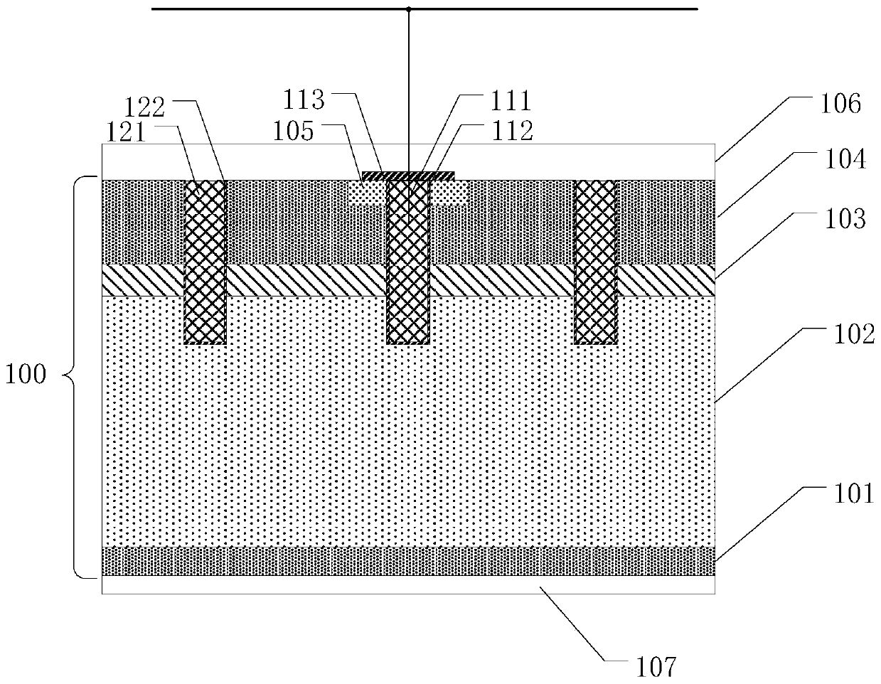
[0064] This embodiment provides a semiconductor device, please refer to figure 2 , figure 2 It is a schematic cross-sectional structure diagram of a semiconductor device according to an embodiment of the present invention, including:
[0065] A semiconductor substrate 200, the semiconductor substrate 200 comprising a first surface and a second surface opposite to the first surface, wherein, figure 2 Wherein, the first surface is defined as the upper surface, and the second surface is defined as the lower surface. A drift region 202 of the first conductivity type is included between the first surface and the second surface, a base region 204 of the second conductivity type is included between the drift region 202 and the first surface, and the drift region A collector region 201 of the second conductivity type is included between 202 and the second surface;
[0066] Specifically, in this embodiment, a charge accumulation layer 203 of the first conductivity type is further...
Embodiment 2
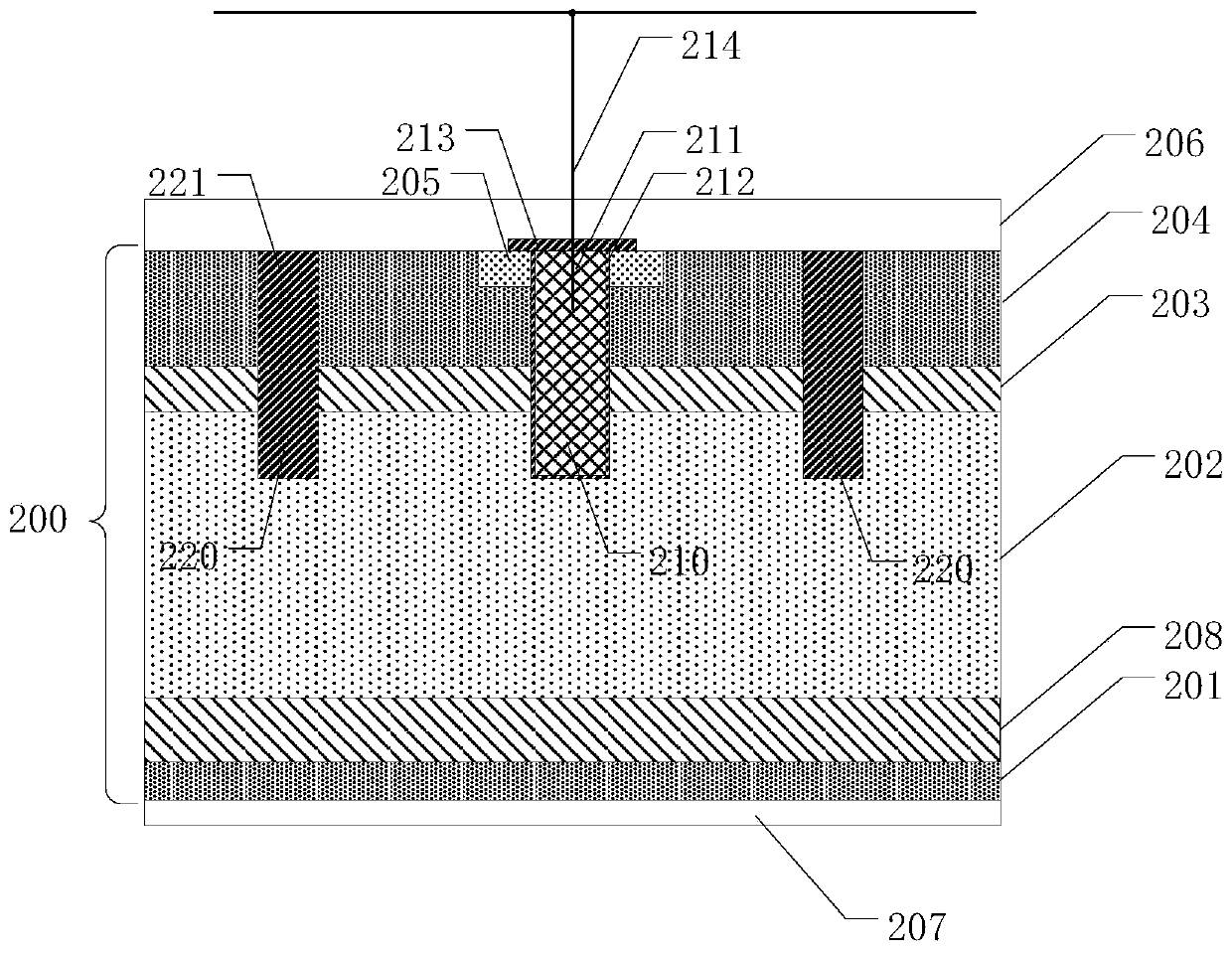
[0076] This embodiment provides a semiconductor device, please refer to image 3 , image 3 It is a schematic cross-sectional structure diagram of a semiconductor device according to an embodiment of the present invention.
[0077] In this embodiment, the semiconductor device includes:
[0078] A semiconductor substrate 300, the semiconductor substrate 300 includes a first surface and a second surface opposite to the first surface, in image 3 Wherein, the first surface is the upper surface of the semiconductor substrate, and the second surface is the lower surface of the semiconductor substrate. A drift region 302 of the first conductivity type is included between the first surface and the second surface, a base region 304 of the second conductivity type is included between the drift region and the first surface, and the drift region and A collector region 301 of the second conductivity type is included between the second surfaces;
[0079] Specifically, in this embodimen...
Embodiment 3
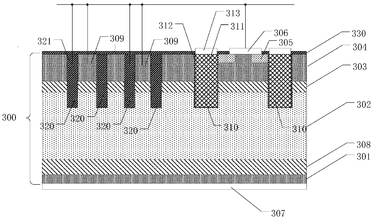
[0093] This embodiment provides a method for forming a semiconductor device, such as Figure 4 As shown, it is a flow chart of the method for forming a semiconductor device in this embodiment, including:
[0094] Step 101: Provide a semiconductor substrate, the semiconductor substrate includes a first surface and a second surface opposite to the first surface, and the drift between the first surface and the second surface includes a first conductivity type a region comprising a base region of a second conductivity type between the drift region and the first surface, and a collector region of the second conductivity type between the drift region and the second surface;
[0095] Step 102: forming a plurality of first trenches and second trenches penetrating through the base region on the first surface of the semiconductor substrate;
[0096] Step 103: filling the second trench with a dielectric material;
[0097] Step 104: forming an isolation layer and a gate material in the ...
PUM
 Abstract
Description
Claims
Application Information
 - Generate Ideas
- Intellectual Property
- Life Sciences
- Materials
- Tech Scout
- Unparalleled Data Quality
- Higher Quality Content
- 60% Fewer Hallucinations
Browse by: Latest US Patents, China's latest patents, Technical Efficacy Thesaurus, Application Domain, Technology Topic, Popular Technical Reports.
© 2025 PatSnap. All rights reserved.Legal|Privacy policy|Modern Slavery Act Transparency Statement|Sitemap|About US| Contact US: help@patsnap.com