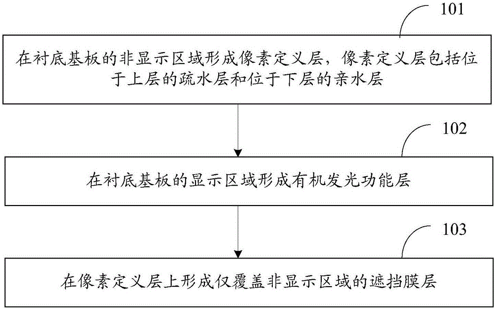
Display substrate and manufacturing method thereof
A display substrate and manufacturing method technology, applied in semiconductor/solid-state device manufacturing, electrical components, electrical solid-state devices, etc., can solve problems such as curved shape, uneven light emission in the inner edge area of pixels, and affect the light-emitting performance of the device, so as to improve light emission Performance, the effect of improving the phenomenon of uneven light emission
- Summary
- Abstract
- Description
- Claims
- Application Information
AI Technical Summary
Problems solved by technology
Method used
Image


Examples
Embodiment Construction
[0035] The following will clearly and completely describe the technical solutions in the embodiments of the present invention with reference to the accompanying drawings in the embodiments of the present invention. Obviously, the described embodiments are only some, not all, embodiments of the present invention. Based on the embodiments of the present invention, all other embodiments obtained by persons of ordinary skill in the art without making creative efforts belong to the protection scope of the present invention.
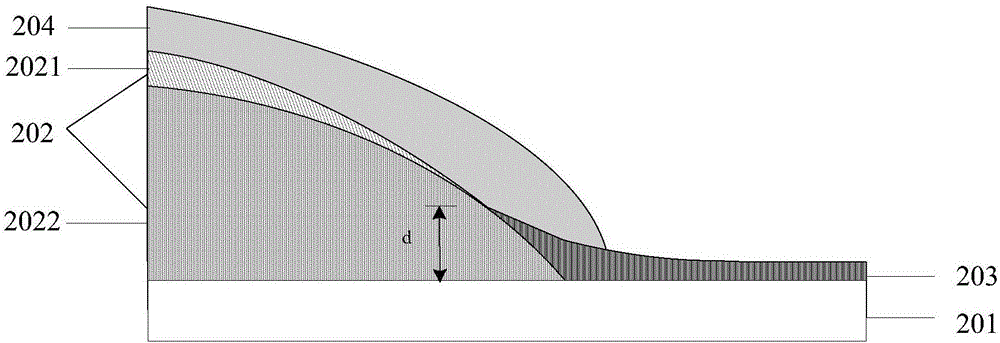
[0036] Wherein, the thickness of the film and the shape of the area in the drawings do not reflect the real scale, and the purpose is only to illustrate the content of the present invention.
[0037] The display substrate provided by the embodiment of the present invention is mainly aimed at the OLED substrate. On the basis of the existing display substrate, the pixel definition layer located in the non-display area is improved, and a blocking film layer is add...
PUM
| Property | Measurement | Unit |
|---|---|---|
| Thickness | aaaaa | aaaaa |
Abstract
Description
Claims
Application Information
 - R&D
- Intellectual Property
- Life Sciences
- Materials
- Tech Scout
- Unparalleled Data Quality
- Higher Quality Content
- 60% Fewer Hallucinations
Browse by: Latest US Patents, China's latest patents, Technical Efficacy Thesaurus, Application Domain, Technology Topic, Popular Technical Reports.
© 2025 PatSnap. All rights reserved.Legal|Privacy policy|Modern Slavery Act Transparency Statement|Sitemap|About US| Contact US: help@patsnap.com