A kind of oled display device and manufacturing method thereof

A display device and pixel technology, applied in semiconductor/solid-state device manufacturing, semiconductor devices, electrical components, etc., can solve the problem of light-emitting pixels stealing light, and achieve the effect of improving product yield

Active Publication Date: 2020-02-11
WUHAN TIANMA MICRO ELECTRONICS CO LTD +1
View PDF4 Cites 0 Cited by
  • Summary
  • Abstract
  • Description
  • Claims
  • Application Information

AI Technical Summary

Problems solved by technology

Due to the good conductivity of the hole injection layer and the hole transport layer, when controlling the light emission of a certain light-emitting pixel, the holes flow from the anode to the cathode, and at the same time, a lateral leakage current will be generated, passing through the hole transport layer and the hole The injection layer reaches adjacent light-emitting pixels, causing other color light-emitting pixels to steal light

Method used


Image

  • A kind of oled display device and manufacturing method thereof
  • A kind of oled display device and manufacturing method thereof
  • A kind of oled display device and manufacturing method thereof

Examples


Embodiment Construction

[0033] The following will clearly and completely describe the technical solutions in the embodiments of the present invention with reference to the accompanying drawings in the embodiments of the present invention. Obviously, the described embodiments are only some, not all, embodiments of the present invention. Based on the embodiments of the present invention, all other embodiments obtained by persons of ordinary skill in the art without making creative efforts belong to the protection scope of the present invention.

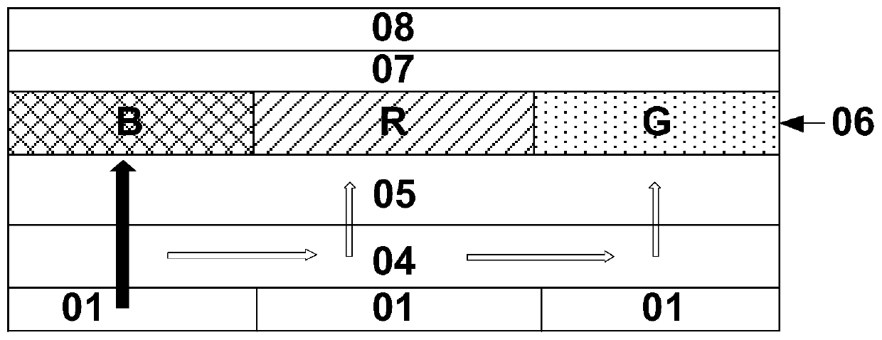
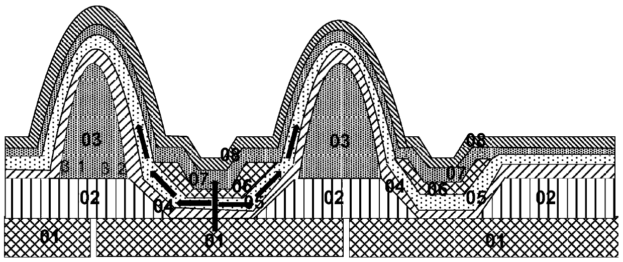
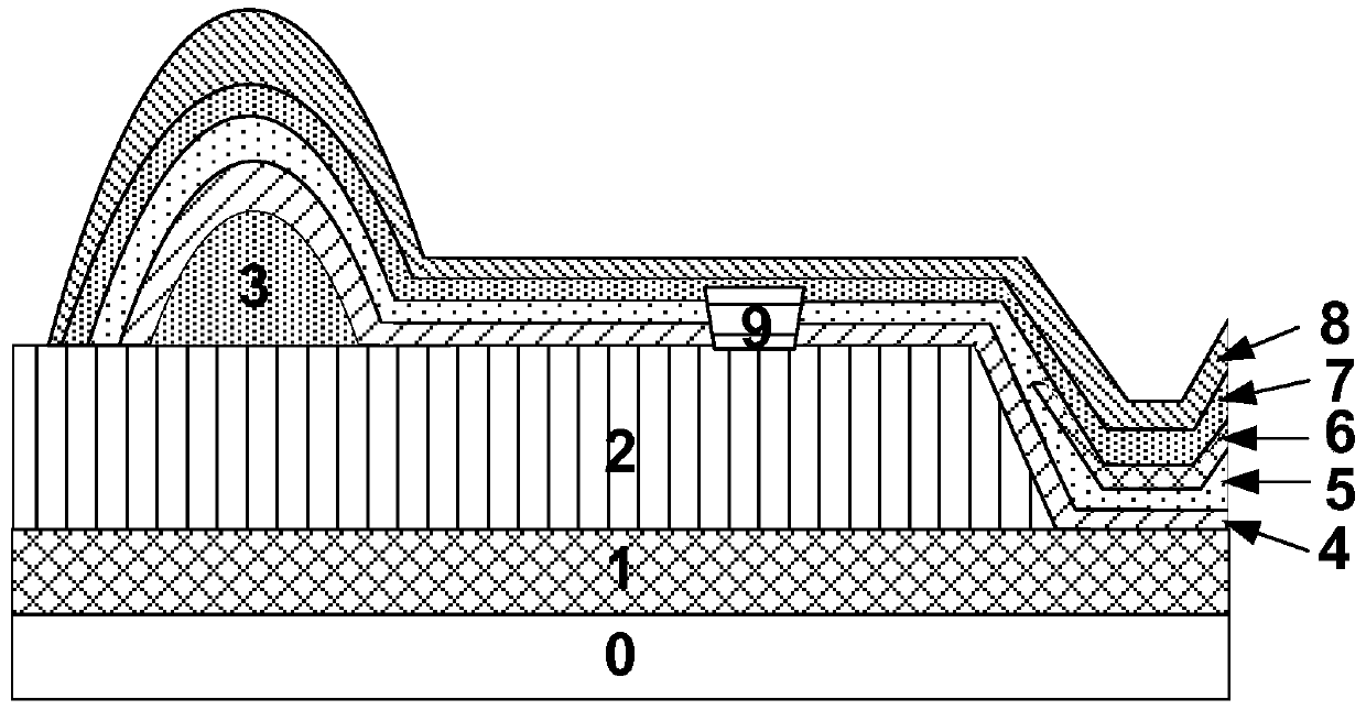
[0034] refer to figure 2 , the OLED display device structure mainly includes: a pixel definition layer for defining light-emitting pixels, and the pixel definition layer includes a pixel area and a pixel interval area 02; spacer columns 03 located above the pixel interval area; and light-emitting pixels; wherein, each Each light emitting pixel includes an anode 01 , a hole injection layer 04 , a hole transport layer 05 , a light emitting layer 06 , an electro...


PUM

PropertyMeasurementUnit
thicknessaaaaaaaaaa

Abstract

The present application discloses an OLED display device and a manufacturing method thereof. The OLED display device includes a substrate, an anode layer, a pixel definition layer, a hole injection layer, a hole transport layer, a light emitting layer, an electron transport layer and an electron injection layer, and a spacer. column; a barrier column located on an area other than the spacer column on the pixel spacing region, the barrier column at least penetrates the hole transport layer and the hole injection layer; in the OLED display device provided by the present invention, in two adjacent color Barrier columns are made on the pixel spacing area between the light-emitting pixels, and at least one of the two internal angles of the barrier column close to the pixel spacing area is greater than 90°, so that when organic materials such as hole transport layers and hole injection layers are evaporated, it is possible to The hole transport layer and the hole injection layer are disconnected at the barrier column, thereby reducing the lateral leakage between a certain light-emitting pixel and adjacent light-emitting pixels when a light-emitting pixel is lit, and preventing other light-emitting pixels from stealing light. Problems, improve product yield.

Description

technical field [0001] The present invention relates to the field of display technology, in particular to an OLED (Organic Light Emitting Diode, Organic Light Emitting Diode) display device and a manufacturing method thereof. Background technique [0002] OLED display technology has the characteristics of self-illumination, the following will refer to figure 1 Describe the structure of a typical OLED display device, figure 1 A structural cross-sectional view of a typical OLED display device is schematically shown. [0003] refer to figure 1 , the OLED display device structure mainly includes a plurality of light-emitting pixels, as shown in the figure R (Red), G (Green), and B (Blue); wherein, each light-emitting pixel includes an anode 01, a hole injection layer 04, a hole A hole transport layer 05 , a light emitting layer 06 , an electron transport layer, an electron injection layer and a cathode 08 . For the convenience of explanation, figure 1 The electron injection...

Claims


Application Information

Patent Timeline
Patent Type & Authority Patents(China)
IPC IPC(8): H01L27/32H01L51/52H01L51/56
CPCH10K59/35H10K50/86H10K71/00
Inventor 臧丹丹熊志勇楚海港
Owner WUHAN TIANMA MICRO ELECTRONICS CO LTD
Why Eureka
Try Eureka