CDM protection circuit structure

A technology for protecting circuits and circuit structures, applied in circuits, electrical components, electric solid devices, etc., can solve the problems of easily damaged gates of PMs and small equivalent impedances

Inactive Publication Date: 2017-05-31
BEIJING CEC HUADA ELECTRONIC DESIGN CO LTD
View PDF3 Cites 2 Cited by
  • Summary
  • Abstract
  • Description
  • Claims
  • Application Information

AI Technical Summary

Problems solved by technology

However, the NW substrate of the PM is connected to the DNW, the gate of the PM is connected to the DC blocking capacitor, ND3 is turned on in the forward direction, and the

Method used


Image

  • CDM protection circuit structure
  • CDM protection circuit structure
  • CDM protection circuit structure

Examples


Embodiment Construction

[0019] In order to make the above-mentioned purposes, features and advantages of the present invention more obvious and easy to understand, the preferred embodiments are exemplified below, and in conjunction with the accompanying drawings, the detailed description is as follows:

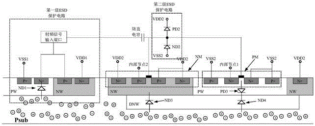
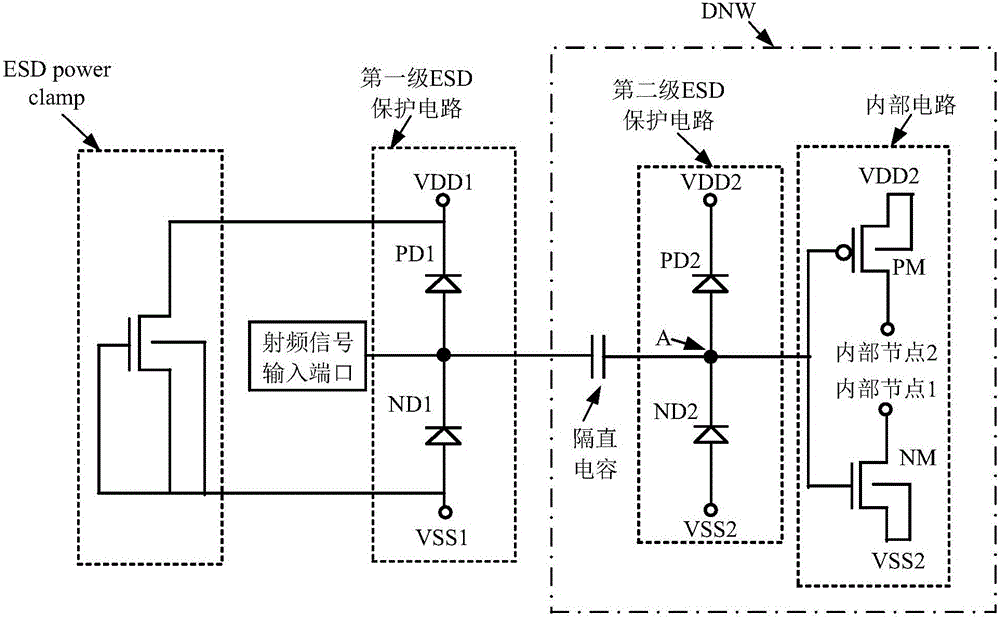
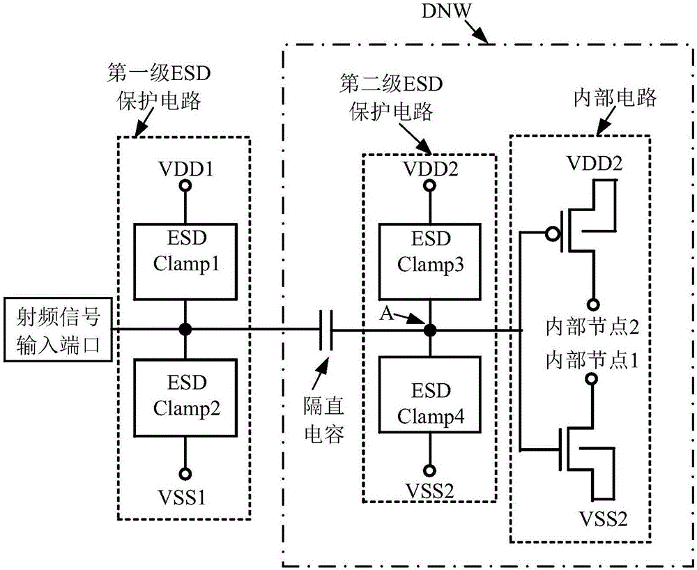
[0020] due to figure 1 In the traditional RF circuit shown, the ESD protection circuit at the RF signal input port cannot provide an ESD discharge path from VDD2 to the DC blocking capacitor, and then to the RF signal input port, so the gate oxide of the PM is easily damaged. The method provided in this embodiment provides such a well-designed path, providing an ESD discharge path from VDD2 to the DC blocking capacitor, and then to the radio frequency signal input port. Such as image 3 As shown, the ESD clamp1 not only has a low-impedance path from the RF signal input port to VDD1, but also provides a low-impedance path from VDD1 to the RF signal input port, and the ESD clamp3 not only has a low-im...


PUM


Abstract

The present invention discloses a CDM (Charged Device Model) protection circuit structure, and is suitable for the design of an ESD (Electro-Static Discharge) protection circuit. The CDM protection circuit structure is characterized in that: the CDM protection circuit structure can improve the CDM protection capacity of a radiofrequency signal input port in a radio frequency circuit, and mainly employs the ESD protection circuit performing dual-way low triggering for a power supply in a first-level ESD protection circuit and employs an ESD protection circuit performing dual-way low triggering for the ground at the same time. The CDM protection circuit structure employs the ESD protection circuit performing dual-way low triggering for the power supply and employs the ESD protection circuit performing dual-way low triggering at the same time in a second-level ESD protection circuit, and in the CDM event, when the radio-frequency signal input port is earthed, the circuit can effectively release the electrostatic charge in the substrate and play the CDM protection effect.

Description

technical field [0001] The invention relates to a CDM protection circuit structure, in particular to a method for improving the CDM protection capability of a radio frequency signal input port in a radio frequency circuit. Background technique [0002] With the increasingly advanced semiconductor technology, the scale of the chip is getting bigger and bigger, and the ESD problems in the process of process processing, transportation, testing and application are getting more and more attention, especially the CDM protection design of large-scale chips. The bottleneck of chip design. [0003] In large-scale chips, the CDM protection design of digital I / O modules is relatively easy to implement, because digital I / O modules usually use high-voltage devices, adopt two-stage ESD protection circuits, and are directly produced and processed on silicon substrates, and CDM discharges The passage is relatively smooth. However, the CDM protection design of the radio frequency port is d...

Claims


Application Information

Patent Timeline
IPC IPC(8): H01L23/60
CPCH01L23/60
Inventor 孙磊孙旭光李志国
Owner BEIJING CEC HUADA ELECTRONIC DESIGN CO LTD
Why Eureka
Try Eureka