Embedded touch screen, manufacturing method thereof and display device

A technology of an in-cell touch screen and a manufacturing method, which can be applied in the directions of instruments, electrical digital data processing, electrical components, etc., can solve the problems of increased overall thickness of OLED devices, high cost, severe water and oxygen conditions, etc., and is conducive to thin and light design. , The effect of reducing production costs and simplifying the production process

Pending Publication Date: 2017-05-31
BOE TECH GRP CO LTD +1
View PDF8 Cites 8 Cited by
  • Summary
  • Abstract
  • Description
  • Claims
  • Application Information

AI Technical Summary

Problems solved by technology

At present, most of the existing OLED-based touch products adopt such as figure 1 In the shown plug-in touch structure, the OLED display panel 01 and the touch panel 02 are made separately, and the two panels are bonded together by the adhesive material 03 to form a complete touch display device. This structure will increase the overall thickness of the OLED device , which is not conducive to the thin and light design of the product
[0003] The in-cell touch screen is to set the touch electrodes inside the display panel, and most of them need to divide and punch the film layer. However, the existing OLED materials are relatively strict with water and oxygen conditions. Therefore, most OLEDs currently use Made by vacuum evaporation process, it is very difficult and expensive to carry out via hole and pattern segmentation process in OLED, which is not conducive to the realization of in-cell touch control in OLED

Method used


Image

  • Embedded touch screen, manufacturing method thereof and display device
  • Embedded touch screen, manufacturing method thereof and display device
  • Embedded touch screen, manufacturing method thereof and display device

Examples


Embodiment Construction

[0039] The specific implementation manners of the in-cell touch screen provided by the embodiments of the present invention, its manufacturing method and the display device will be described in detail below with reference to the accompanying drawings.

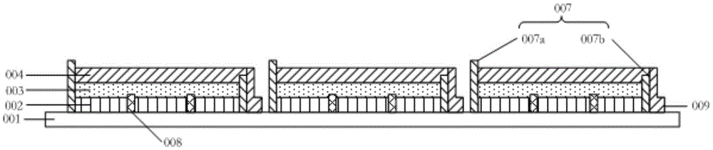
[0040] The thickness and shape of each film layer in the drawings do not reflect the real scale, and the purpose is only to illustrate the content of the present invention.

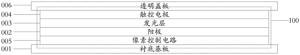
[0041] An embedded touch screen provided by an embodiment of the present invention, such as figure 2 As shown, there are a plurality of electroluminescence sub-pixel regions 100 arranged in a matrix, figure 2 Only one electroluminescent sub-pixel region 100 is shown in the figure, and each electroluminescent sub-pixel region 100 includes: an anode 002 and a light-emitting layer 003 sequentially arranged on a base substrate 001, and also includes:

[0042] A plurality of mutually insulated touch electrodes 004 arranged in a matrix arranged on the light-e...


PUM


Abstract

The invention discloses an embedded touch screen, a manufacturing method thereof and a display device. A plurality of touch electrodes which are matrix-arranged and are insulated from one another are arranged on a luminous layer of an OLED panel; gaps among the tough electrodes are positioned in gaps of electroluminescent sub-pixel regions; and each tough electrode covers at least one electroluminescent sub-pixel region and is used as a cathode of the covered electroluminescent sub-pixel regions. The embedded touch screen provided by an embodiment of the invention is based on the OLED panel, after being divided, the cathodes are used as the touch electrodes to realize embedded touch, therefore, the thickness of a touch display device can be reduced, and lightweight design of the product is facilitated. In addition, when the embedded touch screen based on the OLED panel is manufactured, the cathodes which are used as the touch electrodes are formed in an ink-jet printing mode, a manufacturing process of the touch screen based on the OLED panel can be simplified effectively, and the production cost is reduced.

Description

technical field [0001] The invention relates to the technical field of touch display, in particular to an embedded touch screen, a manufacturing method thereof and a display device. Background technique [0002] Organic light-emitting diodes (OLED) is a display device that is packaged and molded using organic materials. It has the advantages of low operating voltage, fast response speed, high luminous efficiency, wide viewing angle and wide operating temperature. It is beneficial to the thinning, low power consumption and curved surface design of the display device. At present, most of the existing OLED-based touch products use such as figure 1 In the shown plug-in touch structure, the OLED display panel 01 and the touch panel 02 are made respectively, and the two panels are bonded together by the adhesive material 03 to form a complete touch display device. This structure will increase the overall thickness of the OLED device , which is not conducive to the thin and light...

Claims


Application Information

Patent Timeline
IPC IPC(8): G06F3/041H01L27/32
CPCG06F3/0412H10K59/40G06F3/04164G06F3/0443G06F2203/04103H10K50/82G06F3/044H10K59/122H10K71/00H10K71/611H10K59/1201
Inventor 刘伟董学陈小川王海生丁小梁杨盛际刘英明赵卫杰刘红娟李昌峰王鹏鹏
Owner BOE TECH GRP CO LTD
Why Eureka
Try Eureka