
Touch display device and preparation method for same

A touch display and touch sensing layer technology, which is applied in the direction of instrument, electrical digital data processing, and data processing input/output process, etc., can solve problems such as inability to plate touch sensing patterns, polarizers and alignment films that do not have high temperature resistance, etc. , to achieve the effect of saving material and assembly costs, easy single-layer bridging structure, and reducing thickness

Pending Publication Date: 2017-04-05
ANHUI JINGZHUO OPTICAL DISPLAY TECH CO LTD
View PDF3 Cites 8 Cited by
  • Summary
  • Abstract
  • Description
  • Claims
  • Application Information

AI Technical Summary

Problems solved by technology

There are few reports in the industry based on the method of setting a touch-sensitive layer on the polarizer in the display screen and the alignment film in the liquid crystal layer. The main limiting factor is that neither the polarizer nor the alignment film has high temperature resistance, and it cannot The operation of plating touch-sensitive patterns on the surface of the material

Method used


Image

  • Touch display device and preparation method for same
  • Touch display device and preparation method for same
  • Touch display device and preparation method for same

Examples


Embodiment Construction

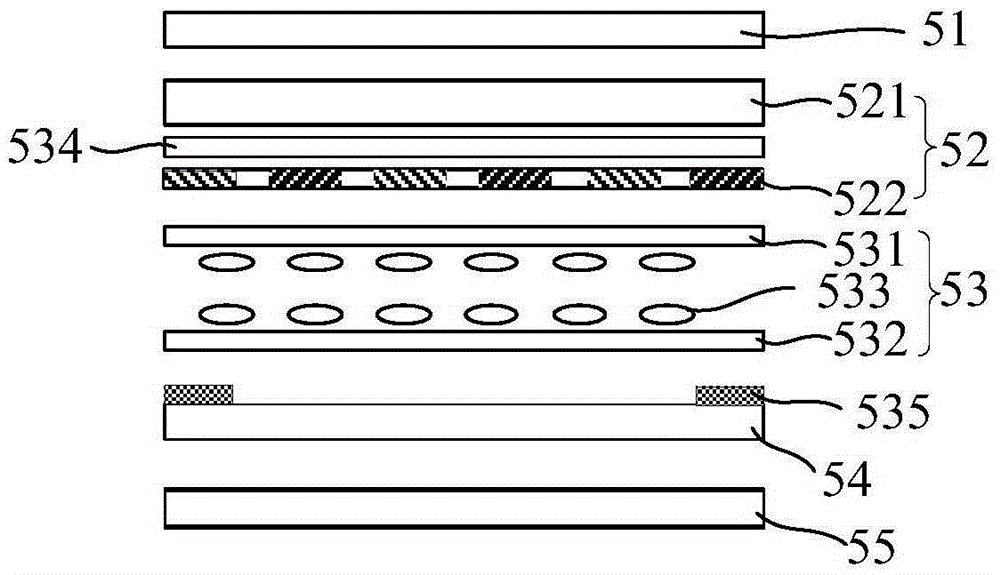
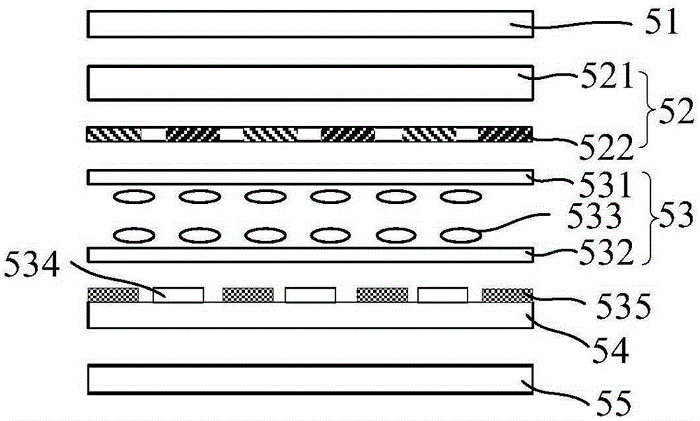
[0032] The touch display device provided by the present invention can be used as a display terminal with a touch interaction form such as a mobile phone and a tablet computer.

[0033] Such as figure 1 As shown, the touch display device includes an upper polarizer 51 , a filter 52 , a liquid crystal layer 53 , a substrate 54 and a lower polarizer 55 arranged in sequence.

[0034] The filter 52 includes a substrate 521 and a filter film 522 disposed on the lower surface of the substrate 521 . The orientation "upper surface" and "lower surface" of related components in the present invention are determined according to how close the touch display device is to the user when its components are in use. "Upper surface" means that the components in the touch display device are close to each other. The surface of the user, the "lower surface" refers to the surface where the elements in the touch display device are away from the user.

[0035] The liquid crystal layer 53 includes an u...


PUM

PropertyMeasurementUnit
Thicknessaaaaaaaaaa

Abstract

The invention relates to a touch display device and a preparation method for the same. The device comprises an upper Polaroid sheet, an optical sheet, a liquid crystal layer, a base plate, a lower Polaroid sheet and a touch sensing layer, wherein the optical sheet is formed by base material and an optical film arranged on the lower surface of the base material; the liquid crystal layer is formed by an upper orientation film, a lower orientation film, liquid crystal clamped between the upper and lower orientation films, and public electrodes and pixel electrodes driving the liquid crystal; the pixel electrode is arranged on the upper surface of the base plate; the touch sensing layer is formed by a polyimides film and a touch control electrode arranged on one surface of the polyimides film; and the touch sensing layer is arranged on the upper and lower surfaces of the upper Polaroid layer, the upper surface of the base material, the lower surface of the optical film, the upper surface of the pixel electrode or the lower surface of the base plate. The touch sensing layer is arranged on elements such as the Polaroid sheets of a display screen, so the display screen has a touch control function and assembly of a touch screen on the display screen is unnecessary; and thickness of the touch display device can be reduced, and material and assembling cost can be reduced.

Description

technical field [0001] The present invention relates to the field of touch display, in particular to a touch display device and a manufacturing method thereof. Background technique [0002] A touch screen is an inductive device that can receive input signals such as touch. The touch screen has endowed information interaction with a new look and is a very attractive new information interaction device. The development of touch screen technology has aroused widespread concern in the information media circles at home and abroad, and has become a rising high-tech industry in the optoelectronic industry. [0003] Currently, electronic devices with a touch display function include a display screen and a touch screen located on the display screen. However, as a component independent from the display screen, the touch screen needs to be ordered according to the size of the display screen when used in some electronic devices for realizing human-computer interaction, and then assembl...

Claims


Application Information

Patent Timeline
IPC IPC(8): G06F3/041
CPCG06F3/0412G06F2203/04103
Inventor 刘伟
Owner ANHUI JINGZHUO OPTICAL DISPLAY TECH CO LTD
Learn More